Our official English website, www.x-mol.net, welcomes your feedback! (Note: you will need to create a separate account there.)
Ultrashort Vertical-Channel van der Waals Semiconductor Transistors.
Advanced Science ( IF 15.1 ) Pub Date : 2019-12-23 , DOI: 10.1002/advs.201902964 Jinbao Jiang 1, 2 , Manh-Ha Doan 2 , Linfeng Sun 2 , Hyun Kim 1, 2 , Hua Yu 1 , Min-Kyu Joo 3 , Sang Hyun Park 1 , Heejun Yang 1, 2 , Dinh Loc Duong 1, 2 , Young Hee Lee 1, 2, 4
Advanced Science ( IF 15.1 ) Pub Date : 2019-12-23 , DOI: 10.1002/advs.201902964 Jinbao Jiang 1, 2 , Manh-Ha Doan 2 , Linfeng Sun 2 , Hyun Kim 1, 2 , Hua Yu 1 , Min-Kyu Joo 3 , Sang Hyun Park 1 , Heejun Yang 1, 2 , Dinh Loc Duong 1, 2 , Young Hee Lee 1, 2, 4
Affiliation
|
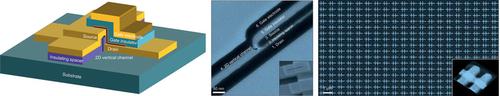
Atomically thin 2D van der Waals semiconductors are promising candidates for next-generation nanoscale field-effect transistors (FETs). Although large-area 2D van der Waals materials have been successfully synthesized, such nanometer-length-scale devices have not been well demonstrated in 2D van der Waals semiconductors. Here, controllable nanometer-scale transistors with a channel length of ≈10 nm are fabricated via vertical channels by squeezing an ultrathin insulating spacer between the out-of-plane source and drain electrodes, and the feasibility of high-density and large-scale fabrication is demonstrated. A large on-current density of ≈70 µA µm-1 nm-1 at a source-drain voltage of 0.5 V and a high on/off ratio of ≈107-109 are obtained in ultrashort 2D vertical channel FETs with monolayer MoS2 synthesized through chemical vapor deposition. The work provides a promising route toward the complementary metal-oxide-semiconductor-compatible fabrication of wafer-scale 2D van der Waals transistors with high-density integration.
中文翻译:

超短垂直通道范德华半导体晶体管。
原子薄的2D范德华半导体是下一代纳米级场效应晶体管(FET)的有希望的候选者。尽管已经成功地合成了大面积的2D Van der Waals材料,但是在2D van der Waals半导体中尚未很好地证明这种纳米级尺寸的器件。在这里,通过挤压平面外源电极和漏电极之间的超薄绝缘间隔物,通过垂直沟道来制造沟道长度约为10 nm的可控纳米级晶体管,以及高密度和大规模制造的可行性被证明。在通过合成单层MoS2的超短2D垂直沟道FET中,在0.5V的源极-漏极电压下获得了约70 µA µm-1 nm-1的大导通电流密度和107-109的高导通/截止比。化学气相沉积。
更新日期:2019-12-23
中文翻译:
超短垂直通道范德华半导体晶体管。
原子薄的2D范德华半导体是下一代纳米级场效应晶体管(FET)的有希望的候选者。尽管已经成功地合成了大面积的2D Van der Waals材料,但是在2D van der Waals半导体中尚未很好地证明这种纳米级尺寸的器件。在这里,通过挤压平面外源电极和漏电极之间的超薄绝缘间隔物,通过垂直沟道来制造沟道长度约为10 nm的可控纳米级晶体管,以及高密度和大规模制造的可行性被证明。在通过合成单层MoS2的超短2D垂直沟道FET中,在0.5V的源极-漏极电压下获得了约70 µA µm-1 nm-1的大导通电流密度和107-109的高导通/截止比。化学气相沉积。


 京公网安备 11010802027423号