当前位置:
X-MOL 学术
›
ACS Photonics
›
论文详情
Our official English website, www.x-mol.net, welcomes your feedback! (Note: you will need to create a separate account there.)
Dark-State-Based Low-Loss Metasurfaces with Simultaneous Electric and Magnetic Resonant Response
ACS Photonics ( IF 7 ) Pub Date : 2019-12-30 , DOI: 10.1021/acsphotonics.9b01480 Aditya Jain 1 , Anthony R. James 2, 3 , John Nogan 2, 3 , Ting S. Luk 2, 3 , Ganapathi Subramania 2, 3 , Sheng Liu 2, 3 , Igal Brener 2, 3 , Nian-Hai Shen 1 , Thomas Koschny 1 , Costas M. Soukoulis 1, 4
ACS Photonics ( IF 7 ) Pub Date : 2019-12-30 , DOI: 10.1021/acsphotonics.9b01480 Aditya Jain 1 , Anthony R. James 2, 3 , John Nogan 2, 3 , Ting S. Luk 2, 3 , Ganapathi Subramania 2, 3 , Sheng Liu 2, 3 , Igal Brener 2, 3 , Nian-Hai Shen 1 , Thomas Koschny 1 , Costas M. Soukoulis 1, 4
Affiliation
|
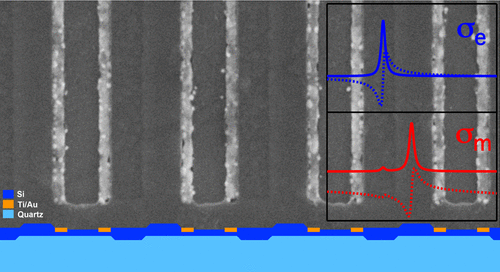
The realization of metamaterials or metasurfaces with simultaneous electric and magnetic response and low loss is generally very challenging at optical frequencies. Traditional approaches using nanoresonators made of noble metals, while suitable for the microwave and terahertz regimes, fail at frequencies above the near-infrared, due to prohibitive high dissipative losses and the breakdown of scaling resulting from the electron mass contribution (kinetic inductance) to the effective reactance of these plasmonic meta-atoms. The alternative route based on Mie resonances of high-index dielectric particles normally leads to structure sizes that tend to break the effective-medium approximation. Here, we propose a subwavelength dark-state-based metasurface, which enables configurable simultaneous electric and magnetic responses with low loss. Proof-of-concept metasurface samples, specifically designed around telecommunication wavelengths (i.e., λ ≈ 1.5 μm), were fabricated and investigated experimentally to validate our theoretical concept. Because the electromagnetic field energy is localized and stored predominantly inside a dark resonant dielectric bound state, the proposed metasurfaces can overcome the loss issue associated with plasmonic resonators made of noble metals and enable scaling to very high operation frequency without suffering from saturation of the resonance frequency due to the kinetic inductance of the electrons.
中文翻译:

基于暗态的低损耗亚表面,具有同时的电和磁共振响应
具有同时的电磁响应和低损耗的超材料或超表面的实现通常在光频率上非常具有挑战性。传统的使用贵金属制成的纳米谐振器的方法虽然适用于微波和太赫兹制,但由于抑制性的高耗散损耗和电子质量对电子的贡献(动力学电感)而导致的氧化皮破坏而无法在高于近红外的频率下失效。这些等离子体质子原子的有效电抗。基于高折射率介电粒子Mie共振的替代途径通常会导致结构尺寸趋于破坏有效介质近似值。在这里,我们提出了一种基于亚波长暗态的超颖表面,该超颖表面能够以低损耗实现可配置的同时电和磁响应。专门设计并围绕电信波长(即λ≈1.5μm)进行概念验证的超表面样本,并进行了实验研究,以验证我们的理论概念。由于电磁场能量主要定位并存储在黑暗的共振介电结合态内,因此所提出的超表面可以克服与贵金属制成的等离子共振器相关的损耗问题,并能够缩放到非常高的工作频率而不会遭受共振频率的饱和由于电子的动感。
更新日期:2019-12-30
中文翻译:
基于暗态的低损耗亚表面,具有同时的电和磁共振响应
具有同时的电磁响应和低损耗的超材料或超表面的实现通常在光频率上非常具有挑战性。传统的使用贵金属制成的纳米谐振器的方法虽然适用于微波和太赫兹制,但由于抑制性的高耗散损耗和电子质量对电子的贡献(动力学电感)而导致的氧化皮破坏而无法在高于近红外的频率下失效。这些等离子体质子原子的有效电抗。基于高折射率介电粒子Mie共振的替代途径通常会导致结构尺寸趋于破坏有效介质近似值。在这里,我们提出了一种基于亚波长暗态的超颖表面,该超颖表面能够以低损耗实现可配置的同时电和磁响应。专门设计并围绕电信波长(即λ≈1.5μm)进行概念验证的超表面样本,并进行了实验研究,以验证我们的理论概念。由于电磁场能量主要定位并存储在黑暗的共振介电结合态内,因此所提出的超表面可以克服与贵金属制成的等离子共振器相关的损耗问题,并能够缩放到非常高的工作频率而不会遭受共振频率的饱和由于电子的动感。


 京公网安备 11010802027423号