当前位置:
X-MOL 学术
›
Nat. Nanotechnol.
›
论文详情
Our official English website, www.x-mol.net, welcomes your feedback! (Note: you will need to create a separate account there.)
Evaporated tellurium thin films for p-type field-effect transistors and circuits.
Nature Nanotechnology ( IF 38.3 ) Pub Date : 2019-12-16 , DOI: 10.1038/s41565-019-0585-9 Chunsong Zhao 1, 2, 3 , Chaoliang Tan 1, 2 , Der-Hsien Lien 1, 2 , Xiaohui Song 3, 4 , Matin Amani 1, 2 , Mark Hettick 1, 2 , Hnin Yin Yin Nyein 1, 2, 3 , Zhen Yuan 1, 2 , Lu Li 1, 2 , Mary C Scott 3, 4 , Ali Javey 1, 2
Nature Nanotechnology ( IF 38.3 ) Pub Date : 2019-12-16 , DOI: 10.1038/s41565-019-0585-9 Chunsong Zhao 1, 2, 3 , Chaoliang Tan 1, 2 , Der-Hsien Lien 1, 2 , Xiaohui Song 3, 4 , Matin Amani 1, 2 , Mark Hettick 1, 2 , Hnin Yin Yin Nyein 1, 2, 3 , Zhen Yuan 1, 2 , Lu Li 1, 2 , Mary C Scott 3, 4 , Ali Javey 1, 2
Affiliation
|
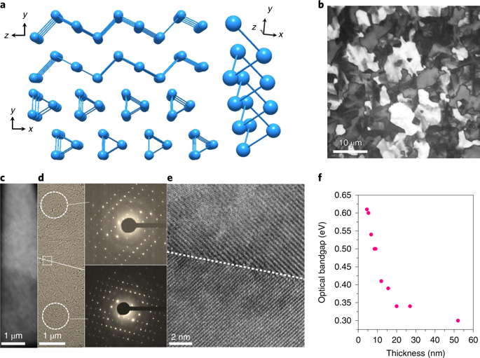
There is an emerging need for semiconductors that can be processed at near ambient temperature with high mobility and device performance. Although multiple n-type options have been identified, the development of their p-type counterparts remains limited. Here, we report the realization of tellurium thin films through thermal evaporation at cryogenic temperatures for fabrication of high-performance wafer-scale p-type field-effect transistors. We achieve an effective hole mobility of ~35 cm2 V-1 s-1, on/off current ratio of ~104 and subthreshold swing of 108 mV dec-1 on an 8-nm-thick film. High-performance tellurium p-type field-effect transistors are fabricated on a wide range of substrates including glass and plastic, further demonstrating the broad applicability of this material. Significantly, three-dimensional circuits are demonstrated by integrating multi-layered transistors on a single chip using sequential lithography, deposition and lift-off processes. Finally, various functional logic gates and circuits are demonstrated.
中文翻译:

用于 p 型场效应晶体管和电路的蒸发碲薄膜。
对能够在接近环境温度下加工且具有高迁移率和器件性能的半导体的需求正在出现。尽管已经确定了多种 n 型选项,但其 p 型对应物的开发仍然有限。在这里,我们报告了在低温下通过热蒸发实现碲薄膜,用于制造高性能晶圆级 p 型场效应晶体管。我们在 8 纳米厚的薄膜上实现了 ~35 cm2 V-1 s-1 的有效空穴迁移率、~104 的开/关电流比和 108 mV dec-1 的亚阈值摆幅。高性能碲 p 型场效应晶体管可在包括玻璃和塑料在内的各种基板上制造,进一步证明了这种材料的广泛适用性。显着地,通过使用顺序光刻、沉积和剥离工艺在单个芯片上集成多层晶体管来演示三维电路。最后,演示了各种功能逻辑门和电路。
更新日期:2019-12-17
中文翻译:
用于 p 型场效应晶体管和电路的蒸发碲薄膜。
对能够在接近环境温度下加工且具有高迁移率和器件性能的半导体的需求正在出现。尽管已经确定了多种 n 型选项,但其 p 型对应物的开发仍然有限。在这里,我们报告了在低温下通过热蒸发实现碲薄膜,用于制造高性能晶圆级 p 型场效应晶体管。我们在 8 纳米厚的薄膜上实现了 ~35 cm2 V-1 s-1 的有效空穴迁移率、~104 的开/关电流比和 108 mV dec-1 的亚阈值摆幅。高性能碲 p 型场效应晶体管可在包括玻璃和塑料在内的各种基板上制造,进一步证明了这种材料的广泛适用性。显着地,通过使用顺序光刻、沉积和剥离工艺在单个芯片上集成多层晶体管来演示三维电路。最后,演示了各种功能逻辑门和电路。


 京公网安备 11010802027423号