当前位置:
X-MOL 学术
›
Nat. Nanotechnol.
›
论文详情
Our official English website, www.x-mol.net, welcomes your feedback! (Note: you will need to create a separate account there.)
A high-performance topological bulk laser based on band-inversion-induced reflection.
Nature Nanotechnology ( IF 38.3 ) Pub Date : 2019-12-16 , DOI: 10.1038/s41565-019-0584-x Zeng-Kai Shao 1, 2, 3 , Hua-Zhou Chen 1, 2, 3 , Suo Wang 1, 2, 3 , Xin-Rui Mao 1, 2, 3 , Zhen-Qian Yang 1, 2, 3 , Shao-Lei Wang 1 , Xing-Xiang Wang 4, 5 , Xiao Hu 4, 5 , Ren-Min Ma 1, 2, 3
Nature Nanotechnology ( IF 38.3 ) Pub Date : 2019-12-16 , DOI: 10.1038/s41565-019-0584-x Zeng-Kai Shao 1, 2, 3 , Hua-Zhou Chen 1, 2, 3 , Suo Wang 1, 2, 3 , Xin-Rui Mao 1, 2, 3 , Zhen-Qian Yang 1, 2, 3 , Shao-Lei Wang 1 , Xing-Xiang Wang 4, 5 , Xiao Hu 4, 5 , Ren-Min Ma 1, 2, 3
Affiliation
|
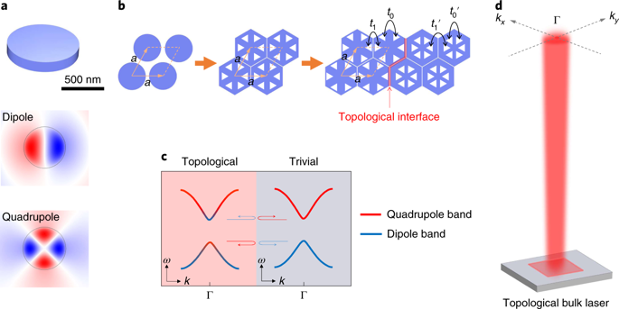
Topological insulators are materials that behave as insulators in the bulk and as conductors at the edge or surface due to the particular configuration of their bulk band dispersion. However, up to date possible practical applications of this band topology on materials' bulk properties have remained abstract. Here, we propose and experimentally demonstrate a topological bulk laser. We pattern semiconductor nanodisk arrays to form a photonic crystal cavity showing topological band inversion between its interior and cladding area. In-plane light waves are reflected at topological edges forming an effective cavity feedback for lasing. This band-inversion-induced reflection mechanism induces single-mode lasing with directional vertical emission. Our topological bulk laser works at room temperature and reaches the practical requirements in terms of cavity size, threshold, linewidth, side-mode suppression ratio and directionality for most practical applications according to Institute of Electrical and Electronics Engineers and other industry standards. We believe this bulk topological effect will have applications in near-field spectroscopy, solid-state lighting, free-space optical sensing and communication.
中文翻译:

基于能带反转诱导反射的高性能拓扑体激光器。
拓扑绝缘体是由于其体能带色散的特定配置而在体中表现为绝缘体并在边缘或表面表现为导体的材料。然而,迄今为止,这种带拓扑结构在材料体积特性上的可能实际应用仍然是抽象的。在这里,我们提出并实验证明了拓扑体激光器。我们图案化半导体纳米盘阵列以形成光子晶体腔,显示其内部和包层区域之间的拓扑带反转。平面内光波在拓扑边缘反射,形成有效的激光腔反馈。这种带反转诱导的反射机制会诱导具有定向垂直发射的单模激光。我们的拓扑体激光器在室温下工作,在腔尺寸、阈值、线宽、边模抑制比和方向性方面达到了大多数实际应用的实际要求,符合电气和电子工程师协会和其他行业标准。我们相信这种体拓扑效应将应用于近场光谱、固态照明、自由空间光学传感和通信。
更新日期:2019-12-17
中文翻译:
基于能带反转诱导反射的高性能拓扑体激光器。
拓扑绝缘体是由于其体能带色散的特定配置而在体中表现为绝缘体并在边缘或表面表现为导体的材料。然而,迄今为止,这种带拓扑结构在材料体积特性上的可能实际应用仍然是抽象的。在这里,我们提出并实验证明了拓扑体激光器。我们图案化半导体纳米盘阵列以形成光子晶体腔,显示其内部和包层区域之间的拓扑带反转。平面内光波在拓扑边缘反射,形成有效的激光腔反馈。这种带反转诱导的反射机制会诱导具有定向垂直发射的单模激光。我们的拓扑体激光器在室温下工作,在腔尺寸、阈值、线宽、边模抑制比和方向性方面达到了大多数实际应用的实际要求,符合电气和电子工程师协会和其他行业标准。我们相信这种体拓扑效应将应用于近场光谱、固态照明、自由空间光学传感和通信。


 京公网安备 11010802027423号