当前位置:
X-MOL 学术
›
Adv. Mater. Technol.
›
论文详情
Our official English website, www.x-mol.net, welcomes your feedback! (Note: you will need to create a separate account there.)
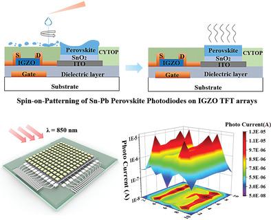
Spin‐On‐Patterning of Sn–Pb Perovskite Photodiodes on IGZO Transistor Arrays for Fast Active‐Matrix Near‐Infrared Imaging
Advanced Materials Technologies ( IF 6.8 ) Pub Date : 2019-12-04 , DOI: 10.1002/admt.201900752 Ya Wang 1 , Changdong Chen 2 , Taoyu Zou 1 , Lizhi Yan 1 , Chuan Liu 2 , Xingzhi Du 1 , Shengdong Zhang 1 , Hang Zhou 1
Advanced Materials Technologies ( IF 6.8 ) Pub Date : 2019-12-04 , DOI: 10.1002/admt.201900752 Ya Wang 1 , Changdong Chen 2 , Taoyu Zou 1 , Lizhi Yan 1 , Chuan Liu 2 , Xingzhi Du 1 , Shengdong Zhang 1 , Hang Zhou 1
Affiliation
|
Flat‐panel imagers have wide applications in industrial and medical inspections. Nonetheless, large area infrared imaging remains a challenge due to the fact that the state‐of‐the‐art infrared sensors are usually based on silicon or germanium technologies, which are limited by the wafer size. Recent advances in low bandgap Sn–Pb perovskite photodiodes (PDs) and indium gallium zinc oxide (IGZO) thin‐film transistors (TFTs) matrix backplane bring new opportunity for developing the large area near‐infrared image sensor. As a proof of concept, a 12 × 12 pixels array with each pixel independently controlled by the gate voltage of a TFT are constructed. Arrays of Sn–Pb based perovskite PDs are spin deposited onto the IGZO TFT drain electrode via self‐assembled patterning process. The low bandgap perovskite PD exhibits a broad spectral response for wavelength from 300 to 1000 nm, featuring a high light to the dark current ratio of ≈104, and a high specific detectivity (D*) of ≈1011 Jones at 850 nm (biased at −0.1 V). The integration takes advantage of the high mobility of IGZO transistors and the high infrared sensitivity of low Sn–Pb perovskite materials, which enables the next generation near‐infrared flat‐panel imager with high frame rate and low operating voltages.
中文翻译:

IGZO晶体管阵列上的Sn-Pb钙钛矿光电二极管的自旋图案化,用于快速有源矩阵近红外成像
平板成像仪在工业和医疗检查中具有广泛的应用。尽管如此,由于最先进的红外传感器通常基于硅或锗技术,这受到晶圆尺寸的限制,因此大面积红外成像仍然是一个挑战。低带隙Sn-Pb钙钛矿光电二极管(PDs)和铟镓锌氧化物(IGZO)薄膜晶体管(TFT)矩阵背板的最新进展为开发大面积近红外图像传感器带来了新的机遇。作为概念证明,构建了一个12×12像素阵列,每个像素由TFT的栅极电压独立控制。通过自组装构图工艺将一系列基于Sn-Pb的钙钛矿PD旋涂到IGZO TFT漏电极上。4,在850 nm处的偏光系数(D *)约为10 11 Jones(在-0.1 V时偏置)。集成利用了IGZO晶体管的高迁移率和低Sn-Pb钙钛矿材料的高红外灵敏度,从而使下一代近红外平板成像器具有高帧频和低工作电压。
更新日期:2020-01-13
中文翻译:
IGZO晶体管阵列上的Sn-Pb钙钛矿光电二极管的自旋图案化,用于快速有源矩阵近红外成像
平板成像仪在工业和医疗检查中具有广泛的应用。尽管如此,由于最先进的红外传感器通常基于硅或锗技术,这受到晶圆尺寸的限制,因此大面积红外成像仍然是一个挑战。低带隙Sn-Pb钙钛矿光电二极管(PDs)和铟镓锌氧化物(IGZO)薄膜晶体管(TFT)矩阵背板的最新进展为开发大面积近红外图像传感器带来了新的机遇。作为概念证明,构建了一个12×12像素阵列,每个像素由TFT的栅极电压独立控制。通过自组装构图工艺将一系列基于Sn-Pb的钙钛矿PD旋涂到IGZO TFT漏电极上。4,在850 nm处的偏光系数(D *)约为10 11 Jones(在-0.1 V时偏置)。集成利用了IGZO晶体管的高迁移率和低Sn-Pb钙钛矿材料的高红外灵敏度,从而使下一代近红外平板成像器具有高帧频和低工作电压。


 京公网安备 11010802027423号