当前位置:
X-MOL 学术
›
Nat. Nanotechnol.
›
论文详情
Our official English website, www.x-mol.net, welcomes your feedback! (Note: you will need to create a separate account there.)
Substrate-directed synthesis of MoS2 nanocrystals with tunable dimensionality and optical properties.
Nature Nanotechnology ( IF 38.3 ) Pub Date : 2019-11-18 , DOI: 10.1038/s41565-019-0571-2 Tomojit Chowdhury 1 , Jungkil Kim 1 , Erick C Sadler 1 , Chenyang Li 2 , Seong Won Lee 3 , Kiyoung Jo 4 , Weinan Xu 5 , David H Gracias 5 , Natalia V Drichko 6 , Deep Jariwala 4 , Todd H Brintlinger 7 , Tim Mueller 2 , Hong-Gyu Park 3 , Thomas J Kempa 1, 2
Nature Nanotechnology ( IF 38.3 ) Pub Date : 2019-11-18 , DOI: 10.1038/s41565-019-0571-2 Tomojit Chowdhury 1 , Jungkil Kim 1 , Erick C Sadler 1 , Chenyang Li 2 , Seong Won Lee 3 , Kiyoung Jo 4 , Weinan Xu 5 , David H Gracias 5 , Natalia V Drichko 6 , Deep Jariwala 4 , Todd H Brintlinger 7 , Tim Mueller 2 , Hong-Gyu Park 3 , Thomas J Kempa 1, 2
Affiliation
|
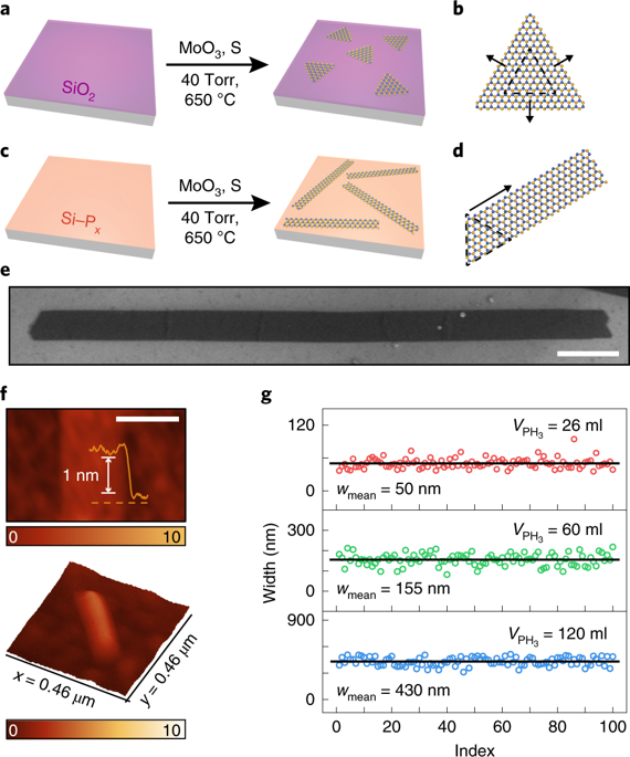
Two-dimensional transition-metal dichalcogenide (TMD) crystals are a versatile platform for optoelectronic, catalytic and quantum device studies. However, the ability to tailor their physical properties through explicit synthetic control of their morphology and dimensionality is a major challenge. Here we demonstrate a gas-phase synthesis method that substantially transforms the structure and dimensionality of TMD crystals without lithography. Synthesis of MoS2 on Si(001) surfaces pre-treated with phosphine yields high-aspect-ratio nanoribbons of uniform width. We systematically control the width of these nanoribbons between 50 and 430 nm by varying the total phosphine dosage during the surface treatment step. Aberration-corrected electron microscopy reveals that the nanoribbons are predominantly 2H phase with zig-zag edges and an edge quality that is comparable to, or better than, that of graphene and TMD nanoribbons prepared through conventional top-down processing. Owing to their restricted dimensionality, the nominally one-dimensional MoS2 nanocrystals exhibit photoluminescence 50 meV higher in energy than that from two-dimensional MoS2 crystals. Moreover, this emission is precisely tunable through synthetic control of crystal width. Directed crystal growth on designer substrates has the potential to enable the preparation of low-dimensional materials with prescribed morphologies and tunable or emergent optoelectronic properties.
中文翻译:

具有可调尺寸和光学特性的MoS2纳米晶体的衬底定向合成。
二维过渡金属二硫化碳(TMD)晶体是用于光电,催化和量子器件研究的多功能平台。然而,通过显式合成控制其形态和尺寸来调整其物理性质的能力是一项重大挑战。在这里,我们演示了一种气相合成方法,该方法无需光刻即可实质上改变TMD晶体的结构和尺寸。在用磷化氢预处理的Si(001)表面上合成MoS2,可得到纵横比均匀的高纵横比纳米带。我们通过在表面处理步骤中改变总磷化氢剂量来系统地将这些纳米带的宽度控制在50至430 nm之间。像差校正电子显微镜显示,纳米带主要为2H相,具有锯齿形边缘,其边缘质量与通过常规自上而下的工艺制备的石墨烯和TMD纳米带相当或更好。由于其尺寸受到限制,名义上一维的MoS2纳米晶体显示出比二维MoS2晶体高50 meV的光致发光。此外,可通过综合控制晶体宽度来精确调整此发射。在设计器基板上进行定向晶体生长具有潜力,可以制备具有规定形态和可调谐或紧急光电特性的低维材料。由于其尺寸受到限制,名义上一维的MoS2纳米晶体显示出比二维MoS2晶体高50 meV的光致发光。此外,可通过综合控制晶体宽度来精确调整此发射。在设计器基板上进行定向晶体生长具有潜力,可以制备具有规定形态和可调谐或紧急光电特性的低维材料。由于其尺寸受到限制,名义上一维的MoS2纳米晶体显示出比二维MoS2晶体高50 meV的光致发光。此外,可通过综合控制晶体宽度来精确调整此发射。在设计器基板上进行定向晶体生长具有潜力,可以制备具有规定形态和可调谐或紧急光电特性的低维材料。
更新日期:2019-11-18
中文翻译:
具有可调尺寸和光学特性的MoS2纳米晶体的衬底定向合成。
二维过渡金属二硫化碳(TMD)晶体是用于光电,催化和量子器件研究的多功能平台。然而,通过显式合成控制其形态和尺寸来调整其物理性质的能力是一项重大挑战。在这里,我们演示了一种气相合成方法,该方法无需光刻即可实质上改变TMD晶体的结构和尺寸。在用磷化氢预处理的Si(001)表面上合成MoS2,可得到纵横比均匀的高纵横比纳米带。我们通过在表面处理步骤中改变总磷化氢剂量来系统地将这些纳米带的宽度控制在50至430 nm之间。像差校正电子显微镜显示,纳米带主要为2H相,具有锯齿形边缘,其边缘质量与通过常规自上而下的工艺制备的石墨烯和TMD纳米带相当或更好。由于其尺寸受到限制,名义上一维的MoS2纳米晶体显示出比二维MoS2晶体高50 meV的光致发光。此外,可通过综合控制晶体宽度来精确调整此发射。在设计器基板上进行定向晶体生长具有潜力,可以制备具有规定形态和可调谐或紧急光电特性的低维材料。由于其尺寸受到限制,名义上一维的MoS2纳米晶体显示出比二维MoS2晶体高50 meV的光致发光。此外,可通过综合控制晶体宽度来精确调整此发射。在设计器基板上进行定向晶体生长具有潜力,可以制备具有规定形态和可调谐或紧急光电特性的低维材料。由于其尺寸受到限制,名义上一维的MoS2纳米晶体显示出比二维MoS2晶体高50 meV的光致发光。此外,可通过综合控制晶体宽度来精确调整此发射。在设计器基板上进行定向晶体生长具有潜力,可以制备具有规定形态和可调谐或紧急光电特性的低维材料。


 京公网安备 11010802027423号