当前位置:
X-MOL 学术
›
Adv. Opt. Mater.
›
论文详情
Our official English website, www.x-mol.net, welcomes your feedback! (Note: you will need to create a separate account there.)
Two‐Dimensional GeP‐Based Broad‐Band Optical Switches and Photodetectors
Advanced Optical Materials ( IF 9 ) Pub Date : 2019-11-13 , DOI: 10.1002/adom.201901490 Tongtong Yu 1 , Hongkun Nie 1 , Shanpeng Wang 1, 2 , Baitao Zhang 1, 2 , Shuqi Zhao 1 , Ziming Wang 1 , Jie Qiao 1 , Bing Han 1 , Jingliang He 1, 2 , Xutang Tao 1, 2
Advanced Optical Materials ( IF 9 ) Pub Date : 2019-11-13 , DOI: 10.1002/adom.201901490 Tongtong Yu 1 , Hongkun Nie 1 , Shanpeng Wang 1, 2 , Baitao Zhang 1, 2 , Shuqi Zhao 1 , Ziming Wang 1 , Jie Qiao 1 , Bing Han 1 , Jingliang He 1, 2 , Xutang Tao 1, 2
Affiliation
|
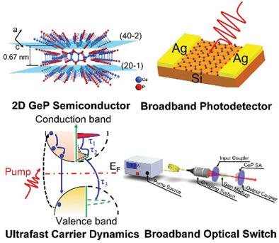
Germanium phosphide (GeP), a typical 2D group IV–V semiconductor, has attracted significant attention due to the advantages of higher thermodynamic stability than black phosphorus (BP), widely tunable bandgap, high carrier mobility, and in‐plane anisotropy. However, its photonic and optoelectronic properties have not been extensively explored so far. Herein, large size and high‐quality GeP single bulk crystal is successfully grown by flux method and stripped into 2D nanosheets with liquid phase exfoliation (LPE) and spin‐coating methods. The broad‐band photonic and optoelectronic properties of 2D GeP nanosheets are systematically investigated. First principles calculations are performed to verify its widely tunable bandgap from 0.43 eV for bulk to 1.58 eV for monolayer. The ultrafast carrier dynamic and non‐linear optical responses are investigated by non‐degenerated pump‐probe and open‐aperture Z‐scan methods, and the results indicate that 2D GeP nanosheets can present excellent broad‐band saturable absorption properties. Furthermore, the 2D GeP nanosheets‐based broad‐band saturable absorbers (SAs) and photodetectors are demonstrated. The results indicate that 2D GeP nanosheets can be used as excellent broad‐band optical modulators and detectors, which will arouse a considerable interest in exploring novel group IV–V 2D materials for broad‐band photonic and optoelectronic applications.
中文翻译:

基于二维GeP的宽带光开关和光电探测器
磷化锗(GeP)是一种典型的二维IV–V族半导体,由于具有比黑磷(BP)高的热力学稳定性,可调节的带隙宽,高的载流子迁移率和面内各向异性等优点而备受关注。但是,迄今为止,尚未对其光子和光电特性进行广泛的研究。在此,大尺寸和高质量的GeP单块晶体通过助熔剂方法成功生长,并通过液相剥落(LPE)和旋涂方法剥离成2D纳米片。系统地研究了二维GeP纳米片的宽带光子和光电特性。进行第一原理计算以验证其广泛可调的带隙(从体积的0.43 eV到单层的1.58 eV)。通过非退化泵浦探针和开孔Z扫描方法研究了超快载流子的动态和非线性光学响应,结果表明2D GeP纳米片可以表现出出色的宽带饱和吸收特性。此外,还演示了基于2D GeP纳米片的宽带可饱和吸收体(SA)和光电探测器。结果表明,二维GeP纳米片可用作出色的宽带光学调制器和检测器,这将引起人们对于探索新颖的IV–V组二维二维材料在宽带光子和光电应用中的兴趣。演示了基于2D GeP纳米片的宽带可饱和吸收体(SA)和光电探测器。结果表明,二维GeP纳米片可用作出色的宽带光学调制器和检测器,这将引起人们对于探索新颖的IV–V组二维二维材料在宽带光子和光电应用中的兴趣。演示了基于2D GeP纳米片的宽带可饱和吸收体(SA)和光电探测器。结果表明,二维GeP纳米片可用作出色的宽带光学调制器和检测器,这将引起人们对于探索新颖的IV–V组二维二维材料在宽带光子和光电应用中的兴趣。
更新日期:2020-01-17
中文翻译:
基于二维GeP的宽带光开关和光电探测器
磷化锗(GeP)是一种典型的二维IV–V族半导体,由于具有比黑磷(BP)高的热力学稳定性,可调节的带隙宽,高的载流子迁移率和面内各向异性等优点而备受关注。但是,迄今为止,尚未对其光子和光电特性进行广泛的研究。在此,大尺寸和高质量的GeP单块晶体通过助熔剂方法成功生长,并通过液相剥落(LPE)和旋涂方法剥离成2D纳米片。系统地研究了二维GeP纳米片的宽带光子和光电特性。进行第一原理计算以验证其广泛可调的带隙(从体积的0.43 eV到单层的1.58 eV)。通过非退化泵浦探针和开孔Z扫描方法研究了超快载流子的动态和非线性光学响应,结果表明2D GeP纳米片可以表现出出色的宽带饱和吸收特性。此外,还演示了基于2D GeP纳米片的宽带可饱和吸收体(SA)和光电探测器。结果表明,二维GeP纳米片可用作出色的宽带光学调制器和检测器,这将引起人们对于探索新颖的IV–V组二维二维材料在宽带光子和光电应用中的兴趣。演示了基于2D GeP纳米片的宽带可饱和吸收体(SA)和光电探测器。结果表明,二维GeP纳米片可用作出色的宽带光学调制器和检测器,这将引起人们对于探索新颖的IV–V组二维二维材料在宽带光子和光电应用中的兴趣。演示了基于2D GeP纳米片的宽带可饱和吸收体(SA)和光电探测器。结果表明,二维GeP纳米片可用作出色的宽带光学调制器和检测器,这将引起人们对于探索新颖的IV–V组二维二维材料在宽带光子和光电应用中的兴趣。


 京公网安备 11010802027423号