Our official English website, www.x-mol.net, welcomes your feedback! (Note: you will need to create a separate account there.)
Tunable quantum dot lasers grown directly on silicon
Optica ( IF 10.4 ) Pub Date : 2019-10-25 , DOI: 10.1364/optica.6.001394 Yating Wan , Sen Zhang , Justin C. Norman , M. J. Kennedy , William He , Songtao Liu , Chao Xiang , Chen Shang , Jian-Jun He , Arthur C. Gossard , John E. Bowers
Optica ( IF 10.4 ) Pub Date : 2019-10-25 , DOI: 10.1364/optica.6.001394 Yating Wan , Sen Zhang , Justin C. Norman , M. J. Kennedy , William He , Songtao Liu , Chao Xiang , Chen Shang , Jian-Jun He , Arthur C. Gossard , John E. Bowers
|
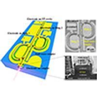
Tunable semiconductor lasers are often listed in critical technology road maps for future dense-wavelength-division-multiplexing (DWDM) systems and high-performance computing systems, and they are increasingly demanded in long-haul, metropolitan, and access networks. The capability to produce such lasers directly on silicon (Si) could boost the use of Si photonics and facilitate the adoption of optical data transmission even at the chip scale. Moreover, just the use of Si as a cheap and large-diameter substrate for device production is very advantageous, as the fabrication can take advantage of the highly optimized processing techniques and economy of scale enabled by decades of development in Si microelectronics. Here, we report a tunable single-wavelength quantum dot (QD) laser directly grown on Si. The high carrier confinement and a real dot density of QDs provide reduced sensitivity to crystalline defects, which allows for exceptional lasing performance even in lattice-mismatched material systems. The discrete density of states of dots yields unique gain properties that show promise for improved device performance and new functionalities relative to the quantum well counterparts, including high temperature stability, low threshold operation, reduced sidewall recombination, and isolator-free stability. We implement a simple, integrable architecture to achieve over 45 dB side-mode-suppression-ratio without involving regrowth steps or subwavelength grating lithography. Under continuous-wave electrical injection at room temperature, we achieved a 16 nm tuning range with output powers of over 2.7 mW per tuning wavelength. This work represents a step towards using III–V/Si epitaxy to form efficient, easily manufacturable on-chip Si light sources for not only DWDM networks, but also spectroscopy, biosensors, and many other emerging applications.
中文翻译:

直接在硅上生长的可调谐量子点激光器
在未来的密集波分复用(DWDM)系统和高性能计算系统的关键技术路线图中,经常会列出可调谐半导体激光器,并且在长途,城域和接入网络中对可调谐半导体激光器的需求也越来越大。直接在硅(Si)上生产此类激光器的能力可以促进Si光子学的使用,甚至在芯片规模上也可以促进采用光学数据传输。而且,仅将Si用作便宜且大直径的衬底用于器件生产是非常有利的,因为制造可以利用由Si微电子学数十年的发展所实现的高度优化的处理技术和规模经济。在这里,我们报告了直接在Si上生长的可调单波长量子点(QD)激光器。高载流子限制和量子点的实际点密度降低了对晶体缺陷的敏感性,即使在晶格不匹配的材料系统中,也可以实现出色的激光性能。点状状态的离散密度产生了独特的增益特性,相对于量子阱同类产品,它们有望改善器件性能并提供新功能,包括高温稳定性,低阈值操作,减少的侧壁重组以及无隔离层的稳定性。我们实现了一种简单,可集成的体系结构,以实现超过45 dB的边模抑制比,而无需涉及再生长步骤或亚波长光栅光刻。在室温下连续波电注入下,我们实现了16 nm的调谐范围,每个调谐波长的输出功率超过2.7 mW。
更新日期:2019-11-21
中文翻译:
直接在硅上生长的可调谐量子点激光器
在未来的密集波分复用(DWDM)系统和高性能计算系统的关键技术路线图中,经常会列出可调谐半导体激光器,并且在长途,城域和接入网络中对可调谐半导体激光器的需求也越来越大。直接在硅(Si)上生产此类激光器的能力可以促进Si光子学的使用,甚至在芯片规模上也可以促进采用光学数据传输。而且,仅将Si用作便宜且大直径的衬底用于器件生产是非常有利的,因为制造可以利用由Si微电子学数十年的发展所实现的高度优化的处理技术和规模经济。在这里,我们报告了直接在Si上生长的可调单波长量子点(QD)激光器。高载流子限制和量子点的实际点密度降低了对晶体缺陷的敏感性,即使在晶格不匹配的材料系统中,也可以实现出色的激光性能。点状状态的离散密度产生了独特的增益特性,相对于量子阱同类产品,它们有望改善器件性能并提供新功能,包括高温稳定性,低阈值操作,减少的侧壁重组以及无隔离层的稳定性。我们实现了一种简单,可集成的体系结构,以实现超过45 dB的边模抑制比,而无需涉及再生长步骤或亚波长光栅光刻。在室温下连续波电注入下,我们实现了16 nm的调谐范围,每个调谐波长的输出功率超过2.7 mW。


 京公网安备 11010802027423号