当前位置:
X-MOL 学术
›
Adv. Mater.
›
论文详情
Our official English website, www.x-mol.net, welcomes your feedback! (Note: you will need to create a separate account there.)
Modulating Epitaxial Atomic Structure of Antimonene through Interface Design
Advanced Materials ( IF 29.4 ) Pub Date : 2019-06-03 , DOI: 10.1002/adma.201902606 Tianchao Niu 1, 2 , Wenhan Zhou 1, 3 , Dechun Zhou 1, 2 , Xuemin Hu 1, 3 , Shengli Zhang 1, 3 , Kan Zhang 1, 3 , Miao Zhou 4 , Harald Fuchs 1, 2, 5 , Haibo Zeng 1, 3
Advanced Materials ( IF 29.4 ) Pub Date : 2019-06-03 , DOI: 10.1002/adma.201902606 Tianchao Niu 1, 2 , Wenhan Zhou 1, 3 , Dechun Zhou 1, 2 , Xuemin Hu 1, 3 , Shengli Zhang 1, 3 , Kan Zhang 1, 3 , Miao Zhou 4 , Harald Fuchs 1, 2, 5 , Haibo Zeng 1, 3
Affiliation
|
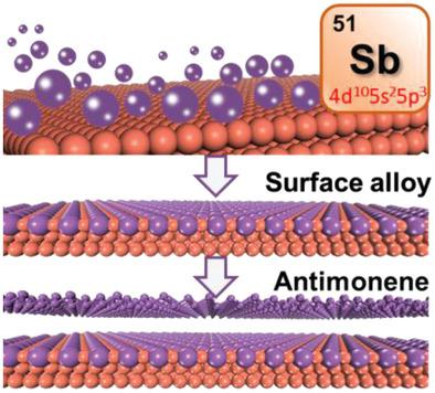
Antimonene, a new semiconductor with fundamental bandgap and desirable stability, has been experimentally realized recently. However, epitaxial growth of wafer‐scale single‐crystalline monolayer antimonene preserving its buckled configuration remains a daunting challenge. Here, Cu(111) and Cu(110) are chosen as the substrates to fabricate high‐quality, single‐crystalline antimonene via molecular beam epitaxy (MBE). Surface alloys form spontaneously after the deposition and postannealing of Sb on two substrates that show threefold and twofold symmetry with different lattice constants. Increasing the coverage leads to the epitaxial growth of two atomic types of antimonene, both exhibiting a hexagonal lattice but with significant difference in lattice constants, which are observed by scanning tunneling microscopy. Scanning tunneling spectroscopy measurements reveal the strain‐induced tunable bandgap, in agreement with the first‐principles calculations. The results show that epitaxial growth of antimonene on different substrates allow the electronic properties of these films to be tuned by substrate‐induced strain and stress.
中文翻译:

通过界面设计调节锑的外延原子结构
最近,通过实验实现了具有基本带隙和期望的稳定性的新型半导体锑。然而,保持其弯曲结构的晶片级单晶单层锑的外延生长仍然是一个艰巨的挑战。在这里,选择Cu(111)和Cu(110)作为衬底,通过分子束外延(MBE)来制造高质量的单晶锑。Sb在两个衬底上沉积和后退火后,会自发形成表面合金,这些衬底表现出三重和两倍对称性,具有不同的晶格常数。通过扫描隧道显微镜观察,增加覆盖率导致两种原子类型的锑的外延生长,二者均显示出六边形晶格,但晶格常数存在显着差异。扫描隧道光谱测量显示出应变引起的可调带隙,与第一性原理计算一致。结果表明,锑在不同衬底上的外延生长可以通过衬底诱导的应变和应力来调节这些薄膜的电子性能。
更新日期:2019-06-03
中文翻译:
通过界面设计调节锑的外延原子结构
最近,通过实验实现了具有基本带隙和期望的稳定性的新型半导体锑。然而,保持其弯曲结构的晶片级单晶单层锑的外延生长仍然是一个艰巨的挑战。在这里,选择Cu(111)和Cu(110)作为衬底,通过分子束外延(MBE)来制造高质量的单晶锑。Sb在两个衬底上沉积和后退火后,会自发形成表面合金,这些衬底表现出三重和两倍对称性,具有不同的晶格常数。通过扫描隧道显微镜观察,增加覆盖率导致两种原子类型的锑的外延生长,二者均显示出六边形晶格,但晶格常数存在显着差异。扫描隧道光谱测量显示出应变引起的可调带隙,与第一性原理计算一致。结果表明,锑在不同衬底上的外延生长可以通过衬底诱导的应变和应力来调节这些薄膜的电子性能。


 京公网安备 11010802027423号