当前位置:
X-MOL 学术
›
J. Phys. Chem. Lett.
›
论文详情
Our official English website, www.x-mol.net, welcomes your feedback! (Note: you will need to create a separate account there.)
Femtosecond Laser-Printed Gold Nanoantennas for Electrically Driven and Bias-Tuned Nanoscale Light Sources Operating in Visible and Infrared Spectral Ranges
The Journal of Physical Chemistry Letters ( IF 5.7 ) Pub Date : 2023-05-30 , DOI: 10.1021/acs.jpclett.3c00650 Denis V Lebedev 1, 2, 3 , Nikita A Solomonov 1 , Liliia N Dvoretckaia 1 , Vitaliy A Shkoldin 1, 4 , Dmitry V Permyakov 4 , Alexander V Arkhipov 5 , Alexey M Mozharov 1 , Dmitry V Pavlov 6 , Aleksandr A Kuchmizhak 6, 7 , Ivan S Mukhin 1, 4, 5
The Journal of Physical Chemistry Letters ( IF 5.7 ) Pub Date : 2023-05-30 , DOI: 10.1021/acs.jpclett.3c00650 Denis V Lebedev 1, 2, 3 , Nikita A Solomonov 1 , Liliia N Dvoretckaia 1 , Vitaliy A Shkoldin 1, 4 , Dmitry V Permyakov 4 , Alexander V Arkhipov 5 , Alexey M Mozharov 1 , Dmitry V Pavlov 6 , Aleksandr A Kuchmizhak 6, 7 , Ivan S Mukhin 1, 4, 5
Affiliation
|
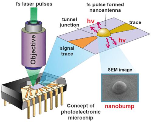
Nanoscale electrically driven light-emitting sources with tunable wavelength represent a milestone for implementation of integrated optoelectronic chips. Plasmonic nanoantennas exhibiting an enhanced local density of optical states (LDOS) and strong Purcell effect hold promise for fabrication of bright nanoscale light emitters. Here, we justify gold parabola-shaped nanobumps and their ordered arrays produced by direct ablation-free femtosecond laser printing as broadband plasmonic light sources electrically excited by a probe of scanning tunneling microscope (STM). I–V curves of the probe-nanoantenna tunnel junction reveal characteristic bias voltages correlating with visible-range localized (0.55 and 0.85 μm) and near-IR (1.65 and 1.87 μm) collective plasmonic modes of these nanoantennas. These multiband resonances confirmed by optical spectroscopy and full-wave simulations provide enhanced LDOS for efficient electrically driven and bias-tuned light emission. Additionally, our studies confirm remarkable applicability of STM for accurate study of optical modes supported by the plasmonic nanoantennas at nanoscale spatial resolution.
中文翻译:

用于在可见光和红外光谱范围内工作的电驱动和偏置调谐纳米级光源的飞秒激光打印金纳米天线
具有可调波长的纳米级电驱动发光源代表了实现集成光电芯片的里程碑。表现出增强的局部光学态密度 (LDOS) 和强 Purcell 效应的等离子体纳米天线有望用于制造明亮的纳米级光发射器。在这里,我们证明了由直接无烧蚀飞秒激光打印产生的金抛物线形纳米凸块及其有序阵列作为由扫描隧道显微镜(STM)探针电激发的宽带等离子体光源。探针-纳米天线隧道结的 I-V 曲线揭示了与这些纳米天线的可见范围局部(0.55 和 0.85 μm)和近红外(1.65 和 1.87 μm)集体等离子体模式相关的特征偏置电压。这些由光谱学和全波模拟证实的多波段共振为高效的电驱动和偏置调谐光发射提供了增强的 LDOS。此外,我们的研究证实了 STM 在纳米级空间分辨率下准确研究等离子体纳米天线支持的光学模式的显着适用性。
更新日期:2023-05-30
中文翻译:
用于在可见光和红外光谱范围内工作的电驱动和偏置调谐纳米级光源的飞秒激光打印金纳米天线
具有可调波长的纳米级电驱动发光源代表了实现集成光电芯片的里程碑。表现出增强的局部光学态密度 (LDOS) 和强 Purcell 效应的等离子体纳米天线有望用于制造明亮的纳米级光发射器。在这里,我们证明了由直接无烧蚀飞秒激光打印产生的金抛物线形纳米凸块及其有序阵列作为由扫描隧道显微镜(STM)探针电激发的宽带等离子体光源。探针-纳米天线隧道结的 I-V 曲线揭示了与这些纳米天线的可见范围局部(0.55 和 0.85 μm)和近红外(1.65 和 1.87 μm)集体等离子体模式相关的特征偏置电压。这些由光谱学和全波模拟证实的多波段共振为高效的电驱动和偏置调谐光发射提供了增强的 LDOS。此外,我们的研究证实了 STM 在纳米级空间分辨率下准确研究等离子体纳米天线支持的光学模式的显着适用性。


 京公网安备 11010802027423号