Nature Nanotechnology ( IF 38.3 ) Pub Date : 2023-05-22 , DOI: 10.1038/s41565-023-01399-y Kwan-Ho Kim 1 , Seyong Oh 2 , Merrilyn Mercy Adzo Fiagbenu 1 , Jeffrey Zheng 3 , Pariasadat Musavigharavi 1, 3 , Pawan Kumar 1 , Nicholas Trainor 4 , Areej Aljarb 5 , Yi Wan 6 , Hyong Min Kim 1 , Keshava Katti 1 , Seunguk Song 1 , Gwangwoo Kim 1 , Zichen Tang 1 , Jui-Han Fu 7 , Mariam Hakami 7 , Vincent Tung 6, 7 , Joan M Redwing 4 , Eric A Stach 3 , Roy H Olsson 1 , Deep Jariwala 1
|
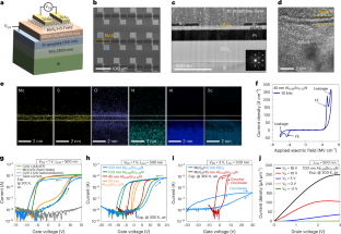
Three-dimensional monolithic integration of memory devices with logic transistors is a frontier challenge in computer hardware. This integration is essential for augmenting computational power concurrent with enhanced energy efficiency in big data applications such as artificial intelligence. Despite decades of efforts, there remains an urgent need for reliable, compact, fast, energy-efficient and scalable memory devices. Ferroelectric field-effect transistors (FE-FETs) are a promising candidate, but requisite scalability and performance in a back-end-of-line process have proven challenging. Here we present back-end-of-line-compatible FE-FETs using two-dimensional MoS2 channels and AlScN ferroelectric materials, all grown via wafer-scalable processes. A large array of FE-FETs with memory windows larger than 7.8 V, ON/OFF ratios greater than 107 and ON-current density greater than 250 μA um–1, all at ~80 nm channel length are demonstrated. The FE-FETs show stable retention up to 10 years by extension, and endurance greater than 104 cycles in addition to 4-bit pulse-programmable memory features, thereby opening a path towards the three-dimensional heterointegration of a two-dimensional semiconductor memory with silicon complementary metal–oxide–semiconductor logic.
中文翻译:
可扩展 CMOS 后端兼容 AlScN/二维通道铁电场效应晶体管
存储器件与逻辑晶体管的三维单片集成是计算机硬件领域的前沿挑战。这种集成对于增强人工智能等大数据应用中的计算能力和能源效率至关重要。尽管经过数十年的努力,仍然迫切需要可靠、紧凑、快速、节能和可扩展的存储设备。铁电场效应晶体管 (FE-FET) 是一种很有前途的候选者,但事实证明,后端工艺中所需的可扩展性和性能具有挑战性。在这里,我们展示了使用二维 MoS 2通道和 AlScN 铁电材料的后端兼容 FE-FET ,所有这些都通过晶圆可扩展工艺生长。展示了存储窗口大于 7.8 V、开/关比大于 10 7以及开电流密度大于 250 μA um –1的大型 FE-FET 阵列,所有通道长度均约为 80 nm。 除了 4 位脉冲可编程存储器功能外,FE-FET 还表现出长达 10 年的稳定保持时间和大于 10 4 个周期的耐用性,从而为二维半导体存储器的三维异质集成开辟了道路具有硅互补金属氧化物半导体逻辑。


 京公网安备 11010802027423号