Nature Materials ( IF 41.2 ) Pub Date : 2023-03-30 , DOI: 10.1038/s41563-023-01520-5 Brian S Y Kim 1, 2 , Aaron J Sternbach 1 , Min Sup Choi 2, 3 , Zhiyuan Sun 1 , Francesco L Ruta 1, 4 , Yinming Shao 1 , Alexander S McLeod 1 , Lin Xiong 1 , Yinan Dong 1 , Ted S Chung 2 , Anjaly Rajendran 2, 5 , Song Liu 2 , Ankur Nipane 5 , Sang Hoon Chae 2, 6 , Amirali Zangiabadi 4 , Xiaodong Xu 7 , Andrew J Millis 1 , P James Schuck 2 , Cory R Dean 1 , James C Hone 2 , D N Basov 1
|
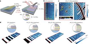
Plasmon polaritons in van der Waals materials hold promise for various photonics applications1,2,3,4. The deterministic imprinting of spatial patterns of high carrier density in plasmonic cavities and nanoscale circuitry can enable the realization of advanced nonlinear nanophotonic5 and strong light–matter interaction platforms6. Here we demonstrate an oxidation-activated charge transfer strategy to program ambipolar low-loss graphene plasmonic structures. By covering graphene with transition-metal dichalcogenides and subsequently oxidizing the transition-metal dichalcogenides into transition-metal oxides, we activate charge transfer rooted in the dissimilar work functions between transition-metal oxides and graphene. Nano-infrared imaging reveals ambipolar low-loss plasmon polaritons at the transition-metal-oxide/graphene interfaces. Further, by inserting dielectric van der Waals spacers, we can precisely control the electron and hole densities induced by oxidation-activated charge transfer and achieve plasmons with a near-intrinsic quality factor. Using this strategy, we imprint plasmonic cavities with laterally abrupt doping profiles with nanoscale precision and demonstrate plasmonic whispering-gallery resonators based on suspended graphene encapsulated in transition-metal oxides.
中文翻译:
双极电荷转移石墨烯等离子体腔
范德华材料中的等离子激元有望用于各种光子学应用1,2,3,4。等离子体腔和纳米级电路中高载流子密度的空间图案的确定性印记可以实现先进的非线性纳米光子5和强光-物质相互作用平台6。在这里,我们展示了一种氧化激活电荷转移策略来编程双极低损耗石墨烯等离子体结构。通过用过渡金属二硫属化物覆盖石墨烯,然后将过渡金属二硫属化物氧化成过渡金属氧化物,我们激活了源于过渡金属氧化物和石墨烯之间不同功函数的电荷转移。纳米红外成像揭示了过渡金属氧化物/石墨烯界面处的双极性低损耗等离子体激元。此外,通过插入电介质范德华间隔物,我们可以精确控制氧化激活电荷转移引起的电子和空穴密度,并实现具有接近本征品质因数的等离子体激元。使用这个策略,


 京公网安备 11010802027423号