当前位置:
X-MOL 学术
›
Nano Lett.
›
论文详情
Our official English website, www.x-mol.net, welcomes your feedback! (Note: you will need to create a separate account there.)
Visualizing Giant Ferroelectric Gating Effects in Large-Scale WSe2/BiFeO3 Heterostructures
Nano Letters ( IF 10.8 ) Pub Date : 2022-11-17 , DOI: 10.1021/acs.nanolett.2c02448 Raphaël Salazar 1 , Sara Varotto 2 , Céline Vergnaud 3 , Vincent Garcia 2 , Stéphane Fusil 2 , Julien Chaste 4 , Thomas Maroutian 4 , Alain Marty 3 , Frédéric Bonell 3 , Debora Pierucci 4 , Abdelkarim Ouerghi 4 , François Bertran 1 , Patrick Le Fèvre 1 , Matthieu Jamet 3 , Manuel Bibes 2 , Julien Rault 1
Nano Letters ( IF 10.8 ) Pub Date : 2022-11-17 , DOI: 10.1021/acs.nanolett.2c02448 Raphaël Salazar 1 , Sara Varotto 2 , Céline Vergnaud 3 , Vincent Garcia 2 , Stéphane Fusil 2 , Julien Chaste 4 , Thomas Maroutian 4 , Alain Marty 3 , Frédéric Bonell 3 , Debora Pierucci 4 , Abdelkarim Ouerghi 4 , François Bertran 1 , Patrick Le Fèvre 1 , Matthieu Jamet 3 , Manuel Bibes 2 , Julien Rault 1
Affiliation
|
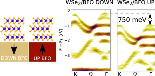
Multilayers based on quantum materials (complex oxides, topological insulators, transition-metal dichalcogenides, etc.) have enabled the design of devices that could revolutionize microelectronics and optoelectronics. However, heterostructures incorporating quantum materials from different families remain scarce, while they would immensely broaden the range of possible applications. Here we demonstrate the large-scale integration of compounds from two highly multifunctional families: perovskite oxides and transition-metal dichalcogenides (TMDs). We couple BiFeO3, a room-temperature multiferroic oxide, and WSe2, a semiconducting two-dimensional material with potential for photovoltaics and photonics. WSe2 is grown by molecular beam epitaxy and transferred on a centimeter-scale onto BiFeO3 films. Using angle-resolved photoemission spectroscopy, we visualize the electronic structure of 1 to 3 monolayers of WSe2 and evidence a giant energy shift as large as 0.75 eV induced by the ferroelectric polarization direction in the underlying BiFeO3. Such a strong shift opens new perspectives in the efficient manipulation of TMD properties by proximity effects.
中文翻译:

可视化大规模 WSe2/BiFeO3 异质结构中的巨大铁电门控效应
基于量子材料(复合氧化物、拓扑绝缘体、过渡金属二硫族化物等)的多层结构使设计的器件能够彻底改变微电子学和光电子学。然而,包含来自不同家族的量子材料的异质结构仍然很少,但它们将极大地拓宽可能的应用范围。在这里,我们展示了来自两个高度多功能家族的化合物的大规模整合:钙钛矿氧化物和过渡金属二硫化物(TMD)。我们将室温下的多铁氧化物 BiFeO 3和具有光伏和光子学潜力的半导体二维材料 WSe 2 结合起来。硒化钨2通过分子束外延生长并以厘米级转移到 BiFeO 3薄膜上。使用角分辨光电子能谱,我们可视化了 1 到 3 个单层 WSe 2的电子结构,并证明了由底层 BiFeO 3中的铁电极化方向引起的高达 0.75 eV 的巨大能量偏移。这种强烈的转变为通过邻近效应有效操纵 TMD 属性开辟了新的视角。
更新日期:2022-11-17
中文翻译:
可视化大规模 WSe2/BiFeO3 异质结构中的巨大铁电门控效应
基于量子材料(复合氧化物、拓扑绝缘体、过渡金属二硫族化物等)的多层结构使设计的器件能够彻底改变微电子学和光电子学。然而,包含来自不同家族的量子材料的异质结构仍然很少,但它们将极大地拓宽可能的应用范围。在这里,我们展示了来自两个高度多功能家族的化合物的大规模整合:钙钛矿氧化物和过渡金属二硫化物(TMD)。我们将室温下的多铁氧化物 BiFeO 3和具有光伏和光子学潜力的半导体二维材料 WSe 2 结合起来。硒化钨2通过分子束外延生长并以厘米级转移到 BiFeO 3薄膜上。使用角分辨光电子能谱,我们可视化了 1 到 3 个单层 WSe 2的电子结构,并证明了由底层 BiFeO 3中的铁电极化方向引起的高达 0.75 eV 的巨大能量偏移。这种强烈的转变为通过邻近效应有效操纵 TMD 属性开辟了新的视角。


 京公网安备 11010802027423号