当前位置:
X-MOL 学术
›
ACS Photonics
›
论文详情
Our official English website, www.x-mol.net, welcomes your feedback! (Note: you will need to create a separate account there.)
Terahertz Nanoimaging of Perovskite Solar Cell Materials
ACS Photonics ( IF 7 ) Pub Date : 2022-10-17 , DOI: 10.1021/acsphotonics.2c00861 Richard H. J. Kim 1 , Zhaoyu Liu 1, 2 , Chuankun Huang 1, 2 , Joong-Mok Park 1 , Samuel J. Haeuser 1, 2 , Zhaoning Song 3 , Yanfa Yan 3 , Yongxin Yao 1 , Liang Luo 1 , Jigang Wang 1, 2
ACS Photonics ( IF 7 ) Pub Date : 2022-10-17 , DOI: 10.1021/acsphotonics.2c00861 Richard H. J. Kim 1 , Zhaoyu Liu 1, 2 , Chuankun Huang 1, 2 , Joong-Mok Park 1 , Samuel J. Haeuser 1, 2 , Zhaoning Song 3 , Yanfa Yan 3 , Yongxin Yao 1 , Liang Luo 1 , Jigang Wang 1, 2
Affiliation
|
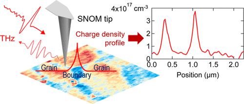
Direct visualization and quantitative evaluation of charge filling in grain boundary (GB) traps of hybrid metal halide perovskites require dynamic conductivity imaging simultaneously at the terahertz (THz) frequency and nanometer (nm) spatial scales not accessible by conventional transport and imaging methods used thus far. Here, we apply a THz near-field nanoconductivity mapping to the archetypal metal halide perovskite photovoltaic films and demonstrate that it is a powerful tool to reveal distinct dielectric heterogeneity due to charge trapping and degradation at the single GB level. Our approach visualizes the filled defect ion traps by local THz charge conductivity and allows for extracting a quantitative profile of trapping density in the vicinity of GBs with sub-20 nm resolution. Furthermore, imaging material degradation by tracking local nanodefect distributions overtime identifies a distinct degradation pathway that starts from the GBs and propagates inside the grains over time. The single GB, nano-THz conductivity imaging demonstrated here can be extended to benchmark various perovskite materials and devices for their global photoenergy conversion performance and local charge transfer proprieties of absorbers and interfaces.
中文翻译:

钙钛矿太阳能电池材料的太赫兹纳米成像
杂化金属卤化物钙钛矿晶界 (GB) 陷阱中电荷填充的直接可视化和定量评估需要在太赫兹 (THz) 频率和纳米 (nm) 空间尺度同时进行动态电导率成像,这是迄今为止使用的传统传输和成像方法无法达到的. 在这里,我们将 THz 近场纳米电导率映射应用于原型金属卤化物钙钛矿光伏薄膜,并证明它是揭示由于单个 GB 水平的电荷捕获和降解而导致的明显介电异质性的有力工具。我们的方法通过局部 THz 电荷电导率可视化填充的缺陷离子阱,并允许以亚 20 nm 的分辨率提取 GB 附近的俘获密度的定量分布。此外,通过跟踪局部纳米缺陷分布来对材料降解进行成像,可以识别出一种独特的降解途径,该途径从 GB 开始,并随着时间的推移在颗粒内部传播。此处展示的单 GB、纳太赫兹电导率成像可以扩展到基准测试各种钙钛矿材料和设备的全局光能转换性能以及吸收器和界面的局部电荷转移特性。
更新日期:2022-10-17
中文翻译:
钙钛矿太阳能电池材料的太赫兹纳米成像
杂化金属卤化物钙钛矿晶界 (GB) 陷阱中电荷填充的直接可视化和定量评估需要在太赫兹 (THz) 频率和纳米 (nm) 空间尺度同时进行动态电导率成像,这是迄今为止使用的传统传输和成像方法无法达到的. 在这里,我们将 THz 近场纳米电导率映射应用于原型金属卤化物钙钛矿光伏薄膜,并证明它是揭示由于单个 GB 水平的电荷捕获和降解而导致的明显介电异质性的有力工具。我们的方法通过局部 THz 电荷电导率可视化填充的缺陷离子阱,并允许以亚 20 nm 的分辨率提取 GB 附近的俘获密度的定量分布。此外,通过跟踪局部纳米缺陷分布来对材料降解进行成像,可以识别出一种独特的降解途径,该途径从 GB 开始,并随着时间的推移在颗粒内部传播。此处展示的单 GB、纳太赫兹电导率成像可以扩展到基准测试各种钙钛矿材料和设备的全局光能转换性能以及吸收器和界面的局部电荷转移特性。


 京公网安备 11010802027423号