当前位置:
X-MOL 学术
›
ACS Photonics
›
论文详情
Our official English website, www.x-mol.net, welcomes your feedback! (Note: you will need to create a separate account there.)
Concurrent Optimization of Diffraction Fields from Binary Phase Mask for Three-Dimensional Nanopatterning
ACS Photonics ( IF 7 ) Pub Date : 2022-10-13 , DOI: 10.1021/acsphotonics.2c01324 Chihun Lee 1 , Gunho Chang 2 , Jaekyung Kim 1 , Gayea Hyun 2 , Gwangmin Bae 2 , Sunae So 1, 3 , Jooyeong Yun 1 , Junhwa Seong 1 , Younghwan Yang 1 , Dong Yong Park 4 , Seokwoo Jeon 2, 5 , Junsuk Rho 1, 6, 7, 8
ACS Photonics ( IF 7 ) Pub Date : 2022-10-13 , DOI: 10.1021/acsphotonics.2c01324 Chihun Lee 1 , Gunho Chang 2 , Jaekyung Kim 1 , Gayea Hyun 2 , Gwangmin Bae 2 , Sunae So 1, 3 , Jooyeong Yun 1 , Junhwa Seong 1 , Younghwan Yang 1 , Dong Yong Park 4 , Seokwoo Jeon 2, 5 , Junsuk Rho 1, 6, 7, 8
Affiliation
|
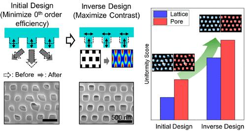
Obtaining a high resolution of a three-dimensional (3D) nanostructure is crucial in nanoengineering. For proximity-field nanopatterning (PnP), a type of nanostructure fabrication with a continuous transfer of interference, the geometry of the phase mask primarily determines the resolution of a fabricated nanostructure by modulating the phase shift of coherent lights. Currently, phase masks for PnP are limited to the intuitive design focusing on reducing zeroth (0th) order efficiency with a single variable design. Herein, the concurrent optimization method, using particle swarm optimization, calculates the optimum phase mask with an improved figure of merit for maximizing the electric field intensity contrast. For the high-contrast 3D nanopatterning, we inversely designed the desired electric-field intensity map and calculated the required phase mask. The calculated optimum phase mask for PnP fabricates the hexagonal nanochannel array with high uniformity in lattice and pore shape owing to its selective intensity control. In contrast to the minimized zeroth diffraction design, which cannot modify the intensity in a specific region, the inverse design can selectively maximize or minimize the intensity in the target regions. This concurrent optimization using the inverse design method increases the degree of freedom for the nanostructure of PnP, and it can fabricate the proper nanostructure applicable to various fields such as energy devices, structural materials, and semiconductor devices.
中文翻译:

三维纳米图案化二元相位掩模衍射场的并行优化
获得三维 (3D) 纳米结构的高分辨率在纳米工程中至关重要。对于近场纳米图案化 (PnP),一种具有连续干涉转移的纳米结构制造,相位掩模的几何形状主要通过调制相干光的相移来确定制造的纳米结构的分辨率。目前,PnP 的相位掩码仅限于直观设计,专注于通过单变量设计降低零阶 (0th) 阶效率。在此,并发优化方法使用粒子群优化,计算具有改进品质因数的最佳相位模板,以最大化电场强度对比度。对于高对比度 3D 纳米图案,我们反向设计了所需的电场强度图并计算了所需的相位模板。由于其选择性强度控制,计算出的 PnP 最佳相位掩模制造了具有高度均匀性的晶格和孔形状的六角形纳米通道阵列。与无法修改特定区域强度的最小化零度衍射设计相比,逆向设计可以选择性地最大化或最小化目标区域中的强度。这种使用逆向设计方法的并行优化增加了PnP纳米结构的自由度,可以制备适用于能源器件、结构材料和半导体器件等各个领域的合适的纳米结构。由于其选择性强度控制,计算出的 PnP 最佳相位掩模制造了具有高度均匀性的晶格和孔形状的六角形纳米通道阵列。与无法修改特定区域强度的最小化零度衍射设计相比,逆向设计可以选择性地最大化或最小化目标区域中的强度。这种使用逆向设计方法的并行优化增加了PnP纳米结构的自由度,可以制备适用于能源器件、结构材料和半导体器件等各个领域的合适的纳米结构。由于其选择性强度控制,计算出的 PnP 最佳相位掩模制造了具有高度均匀性的晶格和孔形状的六角形纳米通道阵列。与无法修改特定区域强度的最小化零度衍射设计相比,逆向设计可以选择性地最大化或最小化目标区域中的强度。这种使用逆向设计方法的并行优化增加了PnP纳米结构的自由度,可以制备适用于能源器件、结构材料和半导体器件等各个领域的合适的纳米结构。逆向设计可以选择性地最大化或最小化目标区域的强度。这种使用逆向设计方法的并行优化增加了PnP纳米结构的自由度,可以制备适用于能源器件、结构材料和半导体器件等各个领域的合适的纳米结构。逆向设计可以选择性地最大化或最小化目标区域的强度。这种使用逆向设计方法的并行优化增加了PnP纳米结构的自由度,可以制备适用于能源器件、结构材料和半导体器件等各个领域的合适的纳米结构。
更新日期:2022-10-13
中文翻译:
三维纳米图案化二元相位掩模衍射场的并行优化
获得三维 (3D) 纳米结构的高分辨率在纳米工程中至关重要。对于近场纳米图案化 (PnP),一种具有连续干涉转移的纳米结构制造,相位掩模的几何形状主要通过调制相干光的相移来确定制造的纳米结构的分辨率。目前,PnP 的相位掩码仅限于直观设计,专注于通过单变量设计降低零阶 (0th) 阶效率。在此,并发优化方法使用粒子群优化,计算具有改进品质因数的最佳相位模板,以最大化电场强度对比度。对于高对比度 3D 纳米图案,我们反向设计了所需的电场强度图并计算了所需的相位模板。由于其选择性强度控制,计算出的 PnP 最佳相位掩模制造了具有高度均匀性的晶格和孔形状的六角形纳米通道阵列。与无法修改特定区域强度的最小化零度衍射设计相比,逆向设计可以选择性地最大化或最小化目标区域中的强度。这种使用逆向设计方法的并行优化增加了PnP纳米结构的自由度,可以制备适用于能源器件、结构材料和半导体器件等各个领域的合适的纳米结构。由于其选择性强度控制,计算出的 PnP 最佳相位掩模制造了具有高度均匀性的晶格和孔形状的六角形纳米通道阵列。与无法修改特定区域强度的最小化零度衍射设计相比,逆向设计可以选择性地最大化或最小化目标区域中的强度。这种使用逆向设计方法的并行优化增加了PnP纳米结构的自由度,可以制备适用于能源器件、结构材料和半导体器件等各个领域的合适的纳米结构。由于其选择性强度控制,计算出的 PnP 最佳相位掩模制造了具有高度均匀性的晶格和孔形状的六角形纳米通道阵列。与无法修改特定区域强度的最小化零度衍射设计相比,逆向设计可以选择性地最大化或最小化目标区域中的强度。这种使用逆向设计方法的并行优化增加了PnP纳米结构的自由度,可以制备适用于能源器件、结构材料和半导体器件等各个领域的合适的纳米结构。逆向设计可以选择性地最大化或最小化目标区域的强度。这种使用逆向设计方法的并行优化增加了PnP纳米结构的自由度,可以制备适用于能源器件、结构材料和半导体器件等各个领域的合适的纳米结构。逆向设计可以选择性地最大化或最小化目标区域的强度。这种使用逆向设计方法的并行优化增加了PnP纳米结构的自由度,可以制备适用于能源器件、结构材料和半导体器件等各个领域的合适的纳米结构。


 京公网安备 11010802027423号