当前位置:
X-MOL 学术
›
Adv. Electron. Mater.
›
论文详情
Our official English website, www.x-mol.net, welcomes your feedback! (Note: you will need to create a separate account there.)
Antimony-Doped p-Type In2Se3 for Heterophase Homojunction with High-Performance Reconfigurable Broadband Photovoltaic Effect
Advanced Electronic Materials ( IF 6.2 ) Pub Date : 2022-08-25 , DOI: 10.1002/aelm.202200665 Shasha Li 1 , Bing Wang 2 , Lixia Li 3 , Jie Li 4 , Mengna Wang 1 , Gaoli Luo 1 , Xiao Ren 2 , Yong Yan 1 , Jingbo Li 1, 4
Advanced Electronic Materials ( IF 6.2 ) Pub Date : 2022-08-25 , DOI: 10.1002/aelm.202200665 Shasha Li 1 , Bing Wang 2 , Lixia Li 3 , Jie Li 4 , Mengna Wang 1 , Gaoli Luo 1 , Xiao Ren 2 , Yong Yan 1 , Jingbo Li 1, 4
Affiliation
|
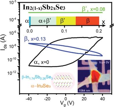
Heterophase homojunction (HH) presents a new paradigm in the next-generation broadband photodetection, light-emitting diode, and nonvolatile memory devices. Lattice mismatch is one of the fundamental characteristics that makes the HH devices difficult to stand out. In2Se3, as a polymorphic layered semiconductor, can provide an effective approach to breaking the critical constraint on interlayer lattice mismatch. However, it is extremely important and challenging to control the crystal phase of In2Se3. In this paper, the phase-selective growth are achieved by alloying antimony (Sb) into In2Se3 crystal structure forming In2(1−x)Sb2xSe3 crystals, where x = 0–20%. Interestingly, for x = 13%, β-In1.74Sb0.26Se3 exhibits a p-type semiconductor characteristic. Accordingly, an α-In2Se3/β-In1.74Sb0.26Se3 van der Waals p–n HH is designed and fabricated. This device not only achieves a broadband spectral photovoltaic response from the visible to near-infrared (405–1064 nm) but also exhibits a fast photoresponse speed at about microseconds at room temperature. Moreover, the photovoltaic figure-of-merits can be greatly modulated by the reconfigurable built-in potential in the p–n HH that is related to the ferroelectric polarization in α-In2Se3. This work enables a great significance of vdW ferroelectric HHs for future photovoltaic and optoelectronic devices.
中文翻译:

用于具有高性能可重构宽带光伏效应的异相同质结的锑掺杂 p 型 In2Se3
异相同质结 (HH) 为下一代宽带光电检测、发光二极管和非易失性存储器件提供了一种新范式。晶格失配是使 HH 器件难以脱颖而出的基本特征之一。In 2 Se 3作为一种多晶型层状半导体,可以提供一种有效的方法来打破层间晶格失配的关键约束。然而,控制In 2 Se 3的晶相是极其重要和具有挑战性的。在本文中,通过将锑 (Sb) 合金化到 In 2 Se 3晶体结构中形成 In 2(1- x ) Sb来实现相选择生长2 x Se 3晶体,其中x = 0–20%。有趣的是,对于x = 13%,β-In 1.74 Sb 0.26 Se 3表现出 p 型半导体特性。因此,α-In 2 Se 3 /β-In 1.74 Sb 0.26 Se 3van der Waals p-n HH 是设计和制造的。该器件不仅实现了从可见光到近红外(405-1064 nm)的宽带光谱光伏响应,而且在室温下表现出约微秒的快速光响应速度。此外,光伏品质因数可以通过与 α-In 2 Se 3中的铁电极化相关的 p-n HH 中可重构的内建电势来极大地调制。这项工作使 vdW 铁电 HHs 对未来的光伏和光电器件具有重要意义。
更新日期:2022-08-25
中文翻译:
用于具有高性能可重构宽带光伏效应的异相同质结的锑掺杂 p 型 In2Se3
异相同质结 (HH) 为下一代宽带光电检测、发光二极管和非易失性存储器件提供了一种新范式。晶格失配是使 HH 器件难以脱颖而出的基本特征之一。In 2 Se 3作为一种多晶型层状半导体,可以提供一种有效的方法来打破层间晶格失配的关键约束。然而,控制In 2 Se 3的晶相是极其重要和具有挑战性的。在本文中,通过将锑 (Sb) 合金化到 In 2 Se 3晶体结构中形成 In 2(1- x ) Sb来实现相选择生长2 x Se 3晶体,其中x = 0–20%。有趣的是,对于x = 13%,β-In 1.74 Sb 0.26 Se 3表现出 p 型半导体特性。因此,α-In 2 Se 3 /β-In 1.74 Sb 0.26 Se 3van der Waals p-n HH 是设计和制造的。该器件不仅实现了从可见光到近红外(405-1064 nm)的宽带光谱光伏响应,而且在室温下表现出约微秒的快速光响应速度。此外,光伏品质因数可以通过与 α-In 2 Se 3中的铁电极化相关的 p-n HH 中可重构的内建电势来极大地调制。这项工作使 vdW 铁电 HHs 对未来的光伏和光电器件具有重要意义。


 京公网安备 11010802027423号