当前位置:
X-MOL 学术
›
Adv. Electron. Mater.
›
论文详情
Our official English website, www.x-mol.net, welcomes your feedback! (Note: you will need to create a separate account there.)
Demonstration of PdSe2 CMOS Using Same Metal Contact in PdSe2 n-/p-MOSFETs through Thickness-Dependent Phase Transition
Advanced Electronic Materials ( IF 6.2 ) Pub Date : 2022-07-20 , DOI: 10.1002/aelm.202200485 Jae Eun Seo 1 , Eunpyo Park 2 , Tanmoy Das 1 , Joon Young Kwak 2 , Jiwon Chang 1
Advanced Electronic Materials ( IF 6.2 ) Pub Date : 2022-07-20 , DOI: 10.1002/aelm.202200485 Jae Eun Seo 1 , Eunpyo Park 2 , Tanmoy Das 1 , Joon Young Kwak 2 , Jiwon Chang 1
Affiliation
|
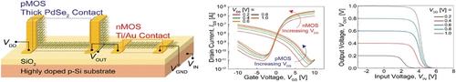
In this study, PdSe2 n- and p-metal-oxide semiconductor field-effect transistors (MOSFETs) are realized using the same conventional metal contact without any doping processes through utilizing the thickness-dependent phase transition in PdSe2. PdSe2 is semiconducting with a sizable band gap in a few layers while semimetallic in bulk. With the thin semiconducting PdSe2 for the channel and the conventional metal source/drain, an n-type behavior is achieved, whereas a p-type behavior with the thin PdSe2 channel and the thick semimetallic PdSe2 source/drain. To understand the carrier injection at the interface between the thin PdSe2 channel and the thick PdSe2 source/drain, a rigorous analysis of the band alignment and the temperature-dependent transfer characteristics is presented to extract the Schottky barrier height at the interface. Additionally, interconnecting PdSe2 n- and p-MOSFETs successfully demonstrate complementary metal-oxide semiconductor (CMOS) inverter with clear voltage transfer characteristics. The proposed approach to control the polarity of PdSe2 MOSFETs using the unique thickness-dependent phase transition in PdSe2 is promising for realizing the CMOS logic circuit with the same channel material and single contact metal.
中文翻译:

通过与厚度相关的相变,在 PdSe2 n-/p-MOSFET 中使用相同金属触点的 PdSe2 CMOS 演示
在这项研究中,通过利用 PdSe 2 中与厚度相关的相变,使用相同的传统金属接触实现了 PdSe 2 n和 p 金属氧化物半导体场效应晶体管 (MOSFET),而无需任何掺杂工艺。PdSe 2是半导电的,在几层中具有相当大的带隙,而在体积上是半金属的。使用薄的半导体 PdSe 2用于沟道和传统的金属源/漏,实现了 n 型行为,而使用薄 PdSe 2沟道和厚的半金属 PdSe 2源/漏实现了 p 型行为。了解薄 PdSe 2通道和厚 PdSe之间界面处的载流子注入2源极/漏极,对能带对齐和与温度相关的传输特性进行了严格分析,以提取界面处的肖特基势垒高度。此外,互连的 PdSe 2 n 和 p MOSFET 成功地展示了具有清晰电压传输特性的互补金属氧化物半导体 (CMOS) 逆变器。所提出的使用 PdSe 2中与厚度相关的独特相变来控制 PdSe 2 MOSFET极性的方法有望用于实现具有相同沟道材料和单一接触金属的 CMOS 逻辑电路。
更新日期:2022-07-20
中文翻译:
通过与厚度相关的相变,在 PdSe2 n-/p-MOSFET 中使用相同金属触点的 PdSe2 CMOS 演示
在这项研究中,通过利用 PdSe 2 中与厚度相关的相变,使用相同的传统金属接触实现了 PdSe 2 n和 p 金属氧化物半导体场效应晶体管 (MOSFET),而无需任何掺杂工艺。PdSe 2是半导电的,在几层中具有相当大的带隙,而在体积上是半金属的。使用薄的半导体 PdSe 2用于沟道和传统的金属源/漏,实现了 n 型行为,而使用薄 PdSe 2沟道和厚的半金属 PdSe 2源/漏实现了 p 型行为。了解薄 PdSe 2通道和厚 PdSe之间界面处的载流子注入2源极/漏极,对能带对齐和与温度相关的传输特性进行了严格分析,以提取界面处的肖特基势垒高度。此外,互连的 PdSe 2 n 和 p MOSFET 成功地展示了具有清晰电压传输特性的互补金属氧化物半导体 (CMOS) 逆变器。所提出的使用 PdSe 2中与厚度相关的独特相变来控制 PdSe 2 MOSFET极性的方法有望用于实现具有相同沟道材料和单一接触金属的 CMOS 逻辑电路。


 京公网安备 11010802027423号