当前位置:
X-MOL 学术
›
Adv. Electron. Mater.
›
论文详情
Our official English website, www.x-mol.net, welcomes your feedback! (Note: you will need to create a separate account there.)
Development of Low-Temperature Doping Process in CdSe-Nanocrystal Thin Films for Flexible Electronic and Optoelectronic Devices
Advanced Electronic Materials ( IF 6.2 ) Pub Date : 2022-07-13 , DOI: 10.1002/aelm.202200297 Yong Min Lee 1 , Byung Ku Jung 2 , Junhyuk Ahn 2 , Taesung Park 2 , Chanho Shin 3 , Tse Nga Ng 3 , In Soo Kim 4, 5 , Ji‐Hyuk Choi 6 , Soong Ju Oh 2
Advanced Electronic Materials ( IF 6.2 ) Pub Date : 2022-07-13 , DOI: 10.1002/aelm.202200297 Yong Min Lee 1 , Byung Ku Jung 2 , Junhyuk Ahn 2 , Taesung Park 2 , Chanho Shin 3 , Tse Nga Ng 3 , In Soo Kim 4, 5 , Ji‐Hyuk Choi 6 , Soong Ju Oh 2
Affiliation
|
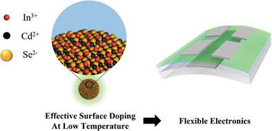
An effective surface-doping strategy for CdSe nanocrystals (NCs) by examining the size-dependency of the doping behavior is introduced. A CdSe NC thin-film transistor (TFT) is fabricated via a doping process with InCl3 treatment followed by an annealing process. Spectroscopic and electronic device characterization reveal that smaller NCs are more effectively doped than larger NCs at all annealing temperatures. This is attributed to the larger specific surface area, where the dopant can be more readily coordinated. The degenerate behavior of a 3.3 nm CdSe-NC TFT appears at a lower temperature than that of larger NC TFTs. High electron mobility and on-to-off current ratio of 1.79 cm2 Vs−1 and 5.2 × 10⁵, respectively are achieved, in a low-temperature annealing process (150 °C) with 3.3 nm CdSe NCs. This facilitates the fabrication of a flexible CdSe-NC TFT, which is demonstrated on a polyethylene terephthalate substrate with an Al2O3 dielectric layer using atomic layer deposition. The flexible 3.3 nm CdSe-NC TFT is successfully fabricated even at 150 °C, with a high on-to-off current ratio and low hysteresis at a low operation voltage, which is impossible for larger CdSe-NC TFTs.
中文翻译:

用于柔性电子和光电器件的 CdSe 纳米晶体薄膜低温掺杂工艺的开发
通过检查掺杂行为的尺寸依赖性,介绍了一种有效的 CdSe 纳米晶体 (NC) 表面掺杂策略。CdSe NC 薄膜晶体管 (TFT) 是通过使用 InCl 3处理的掺杂工艺和退火工艺制造的。光谱和电子器件表征表明,在所有退火温度下,较小的 NC 比较大的 NC 更有效地掺杂。这归因于较大的比表面积,其中掺杂剂可以更容易地配位。3.3 nm CdSe-NC TFT 的退化行为出现在比较大的 NC TFT 更低的温度下。1.79 cm 2 Vs -1和 5.2 × 10 5的高电子迁移率和开关电流比,分别是在具有 3.3 nm CdSe NCs 的低温退火工艺(150 °C)中实现的。这有助于柔性 CdSe-NC TFT 的制造,这在使用原子层沉积的具有 Al 2 O 3介电层的聚对苯二甲酸乙二醇酯基板上进行了演示。柔性 3.3 nm CdSe-NC TFT 即使在 150 °C 下也能成功制造,具有高开关电流比和低工作电压下的低滞后,这对于较大的 CdSe-NC TFT 来说是不可能的。
更新日期:2022-07-13
中文翻译:
用于柔性电子和光电器件的 CdSe 纳米晶体薄膜低温掺杂工艺的开发
通过检查掺杂行为的尺寸依赖性,介绍了一种有效的 CdSe 纳米晶体 (NC) 表面掺杂策略。CdSe NC 薄膜晶体管 (TFT) 是通过使用 InCl 3处理的掺杂工艺和退火工艺制造的。光谱和电子器件表征表明,在所有退火温度下,较小的 NC 比较大的 NC 更有效地掺杂。这归因于较大的比表面积,其中掺杂剂可以更容易地配位。3.3 nm CdSe-NC TFT 的退化行为出现在比较大的 NC TFT 更低的温度下。1.79 cm 2 Vs -1和 5.2 × 10 5的高电子迁移率和开关电流比,分别是在具有 3.3 nm CdSe NCs 的低温退火工艺(150 °C)中实现的。这有助于柔性 CdSe-NC TFT 的制造,这在使用原子层沉积的具有 Al 2 O 3介电层的聚对苯二甲酸乙二醇酯基板上进行了演示。柔性 3.3 nm CdSe-NC TFT 即使在 150 °C 下也能成功制造,具有高开关电流比和低工作电压下的低滞后,这对于较大的 CdSe-NC TFT 来说是不可能的。


 京公网安备 11010802027423号