The European Physical Journal B ( IF 1.6 ) Pub Date : 2022-07-11 , DOI: 10.1140/epjb/s10051-022-00374-1 Li′e Lin, Yangming Cheng, Shuzhen Luo, Xiaoli Cheng, Jinbiao Yang, Wenhu Liao
|
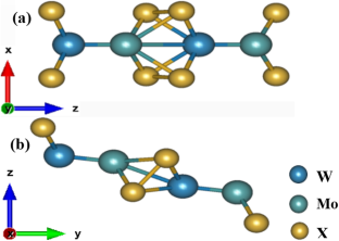
We have investigated the electronic structure and transport properties of the transition metal dichalcogenides composite WX2-MoX2 (X≡S, Se, Te) nanowires under the external strain, in the method of the first-principles calculation combining the Density functional theory (DFT) and the Non-equilibrium Green’s function (NEGF). First, we have designed the two terminal electron transport devices based on the stable transition metal dichalcogenides (TMDs) WX2-MoX2 (X≡S, Se, Te) composite nanowires for the first time. Second, the electronic structure and transport properties of the WS2-MoS2 composite nanowire have been demonstrated to be more sensitive to the external strain when compared to that of the composite WSe2/Te2-MoSe2/Te2 nanowires, the external compressive strain may significantly enchance the differential negative resistance (DNR) effect of the WSe2-MoSe2 composite nanowire based device, while the stretch strain should induce the interesting DNR in the WTe2-MoTe2 composite nanowire device. Finally, the obtained results have been physically explained from the integral area of the transmission coefficient in the bias voltage window, and may be of importance in the design of the nanoelectronic devices based on transition metal dichalcogenides composites.
Graphical abstract
The current–voltage characteristic curves of the two terminal a WS2-MoS2, b WSe2-MoSe2, and c WTe2-MoTe2 composite nanowires under the strain of – 7–7%. The pentagram marked (black) solid line indicates the unstrained case, the solid and hollow circle marked (red) dashed lines indicate the 3% and − 3% strain case, the solid and hollow squares marked (blue) dashed-dot lines denote the 5% and − 5% strain case, while the solid and hollow triangles marked (purple) dotted lines illustrate the 7% and − 7% strain case, respectively. The current of the unstrained WS2-MoS2 composite nanowire device is nearly 0 in the bias range of [− 0.2 V, + 0.2 V] while that should decrease with the increase of the bias voltage in the range of [+ 0.8 V, + 1.0 V], the system behaves an interesting negative differential resistance (NDR) effect. Additionally, the device behaves typical semiconducting feature in the whole bias voltage range under the − 3% compressed strain, while the device current should decrease with the increase of the bias voltage at the regime of [± 0.4 V, ± 0.6 V] and [± 0.8 V, ± 1.0 V], respectively, under the 3% stretched strain. The device should behave significant NDR effect in the bias voltage of [± 0.6 V, ± 0.8 V] under the 5% stretched strain, while one observes the NDR effect at bias voltage range of [− 0.8 V, − 1.0 V], [− 0.4 V, − 0.6 V] and [+ 0.4 V, + 1.0 V], respectively, under the 7% stretched strain. Furthermore, as demonstrated in (b), the current–voltage characteristics curve of the two terminal WSe2-MoSe2 composite nanowires electron device under the strain of – 7–7% behaves typical metallic features. The external strain should significantly enhance the NDR effect of the WSe2-MoSe2 composite nanowires electron device, especially in the compressed – 3– − 7% strain cases. Finally, as illustrated in (c), the current–voltage curve of the two terminal WTe2-MoTe2 composite nanowires electron device under the strain of – 7–7% presents the typical semiconducting features. The observed NDR effect of the composite nanowire devices has been physically explained from the transmission spectra and the integral area of the transmission coefficient in the bias voltage window.
中文翻译:
外应变下过渡金属二硫化物复合WX2-MoX2 (X≡S, Se, Te)纳米线的电子传输特性
我们采用结合密度泛函理论的第一性原理计算方法,研究了过渡金属二硫属化物复合WX 2 -MoX 2 (X≡S, Se, Te)纳米线在外应变作用下的电子结构和输运性质( DFT) 和非平衡格林函数 (NEGF)。首先,我们首次设计了基于稳定的过渡金属二硫属化物(TMDs)WX 2 -MoX 2 (X≡S, Se, Te)复合纳米线的两端电子传输器件。二、WS 2 -MoS 2的电子结构和输运性质与复合WSe 2 /Te 2 -MoSe 2 /Te 2纳米线相比,复合纳米线对外部应变更敏感,外部压缩应变可以显着增强微分负电阻(DNR)效应。 WSe 2 -MoSe 2基于复合纳米线的器件,而拉伸应变应在 WTe 2 -MoTe 2中引起有趣的 DNR复合纳米线器件。最后,从偏压窗口中透射系数的积分面积对所得结果进行了物理解释,可能对基于过渡金属二硫属化物复合材料的纳米电子器件的设计具有重要意义。
图形概要
两端a WS 2 -MoS 2、b WSe 2 -MoSe 2和c WTe 2 -MoTe 2复合纳米线在–7-7%应变下的电流-电压特性曲线。五角星标记(黑色)实线表示无应变情况,实心和空心圆圈标记(红色)虚线表示 3% 和 - 3% 应变情况,实心和空心方块标记(蓝色)点划线表示5% 和 - 5% 应变情况,而标有(紫色)虚线的实心和空心三角形分别表示 7% 和 - 7% 应变情况。无拘无束的WS 2的电流-二硫化钼复合纳米线器件在 [− 0.2 V, + 0.2 V] 的偏置范围内几乎为 0,而随着偏置电压在 [+ 0.8 V, + 1.0 V] 范围内的增加,该值应减小,系统表现出有趣的负差分电阻 (NDR) 效应。此外,该器件在 - 3% 压缩应变下的整个偏置电压范围内表现出典型的半导体特性,而在 [± 0.4 V, ± 0.6 V] 和 [ ± 0.8 V、± 1.0 V],分别在 3% 的拉伸应变下。在 5% 的拉伸应变下,器件应在 [± 0.6 V, ± 0.8 V] 的偏置电压下表现出显着的 NDR 效应,而在 [− 0.8 V, − 1.0 V] 的偏置电压范围内观察到 NDR 效应,[ − 0.4 V, − 0.6 V] 和 [+ 0.4 V, + 1.0 V],分别 在 7% 的拉伸应变下。此外,如 (b ),两端WSe 2 -MoSe 2复合纳米线电子器件在– 7-7%应变下的电流-电压特性曲线表现出典型的金属特征。外部应变应显着增强 WSe 2 -MoSe 2复合纳米线电子器件的 NDR 效应,尤其是在压缩的 - 3- - 7% 应变情况下。最后,如(c)所示,两端WTe 2 -MoTe 2的电流-电压曲线复合纳米线电子器件在 – 7-7% 的应变下呈现典型的半导体特征。观察到的复合纳米线器件的 NDR 效应已经从透射光谱和偏置电压窗口中透射系数的积分面积进行了物理解释。


 京公网安备 11010802027423号