当前位置:
X-MOL 学术
›
Acc. Chem. Res.
›
论文详情
Our official English website, www.x-mol.net, welcomes your feedback! (Note: you will need to create a separate account there.)
Directional Damping of Plasmons at Metal–Semiconductor Interfaces
Accounts of Chemical Research ( IF 18.3 ) Pub Date : 2022-06-13 , DOI: 10.1021/acs.accounts.2c00001 Guoning Liu 1, 2 , Yongbing Lou 1 , Yixin Zhao 3 , Clemens Burda 4
Accounts of Chemical Research ( IF 18.3 ) Pub Date : 2022-06-13 , DOI: 10.1021/acs.accounts.2c00001 Guoning Liu 1, 2 , Yongbing Lou 1 , Yixin Zhao 3 , Clemens Burda 4
Affiliation
|
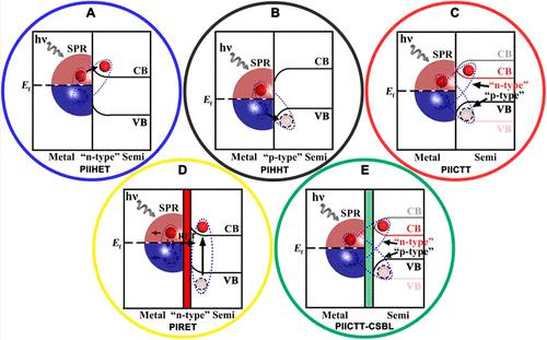
Over the past decade, it has been shown that surface plasmons can enhance photoelectric conversion in photovoltaics, photocatalysis, and other optoelectronic applications through their plasmonic absorption and damping processes. However, plasmonically enhanced devices have yet to routinely match or exceed the efficiencies of traditional semiconductor devices. The effect of plasmonic losses dissipates the absorbed photoenergy mostly into heat and that has hampered the realization of superior next-generation plasmonic optoelectronic devices. Several approaches are being explored to alleviate this situation, including using gain to compensate for the plasmonic losses, designing and synthesizing alternative low-loss plasmonic materials, and reducing activation barriers in plasmonic devices and physical thicknesses of photoabsorber layers to lower the plasmonic losses. A newly proposed plasmon-induced interfacial charge-transfer transition (PIICTT) mechanism has proven to be effective in minimizing energy loss during interfacial charge transfer. The PIICTT leads to a damping of metallic plasmonics by directly generating excitons at the plasmonic metal/semiconductor heteronanostructures. This novel concept has been proven to overcome some of the limitations of electron-transfer inefficiencies, renewing a focus on surface plasmon damping processes with the goal that the plasmonic excitation energies of metal nanoparticles can be more efficiently transferred to the adjacent semiconductor components in the absence and presence of an effective interlayer of carrier-selective blocking layer (CSBL). Several theoretical and experimental studies have concluded that efficient plasmon-induced ultrafast hot-carrier transfer was observed in plasmonic-metal/semiconductor heteronanostructures. The PIICTT mechanism may well be a general phenomenon at plasmonic metal/semiconductor, metal/molecule, semiconductor/semiconductor, and semiconductor/molecule heterointerfaces. Thus, the PIICTT presents a new opportunity to limit energy loss in plasmonic-metal nanostructures and increase device efficiencies based on plasmonic coupling. The nonradiative damping of surface plasmons can impact the energy flux direction and thereby provide a new process beyond light trapping, focusing, and hot carrier creation.
中文翻译:

金属-半导体界面处等离子体的定向阻尼
在过去的十年中,已经表明表面等离子体可以通过其等离子体吸收和阻尼过程来增强光伏、光催化和其他光电应用中的光电转换。然而,等离子体增强器件的效率尚未达到或超过传统半导体器件的效率。等离子体损失的影响将吸收的光能大部分消散为热量,这阻碍了卓越的下一代等离子体光电器件的实现。正在探索几种方法来缓解这种情况,包括使用增益来补偿等离子体损失,设计和合成替代的低损耗等离子体材料,减少等离子体装置中的激活势垒和光吸收层的物理厚度,以降低等离子体损失。一种新提出的等离子体诱导界面电荷转移跃迁 (PIICTT) 机制已被证明可有效减少界面电荷转移过程中的能量损失。PIICTT 通过在等离子金属/半导体异质纳米结构上直接产生激子来导致金属等离子的阻尼。这种新颖的概念已被证明可以克服电子转移效率低下的一些限制,重新关注表面等离子体阻尼过程,目标是在不存在和存在有效的载流子选择性阻挡层 (CSBL) 夹层的情况下,金属纳米粒子的等离子体激发能量可以更有效地转移到相邻的半导体元件。一些理论和实验研究得出结论,在等离子体金属/半导体异质纳米结构中观察到了有效的等离子体诱导的超快热载流子转移。PIICTT 机制很可能是等离子体金属/半导体、金属/分子、半导体/半导体和半导体/分子异质界面的普遍现象。因此,PIICTT 为限制等离子体-金属纳米结构中的能量损失和基于等离子体耦合提高器件效率提供了新的机会。
更新日期:2022-06-13
中文翻译:
金属-半导体界面处等离子体的定向阻尼
在过去的十年中,已经表明表面等离子体可以通过其等离子体吸收和阻尼过程来增强光伏、光催化和其他光电应用中的光电转换。然而,等离子体增强器件的效率尚未达到或超过传统半导体器件的效率。等离子体损失的影响将吸收的光能大部分消散为热量,这阻碍了卓越的下一代等离子体光电器件的实现。正在探索几种方法来缓解这种情况,包括使用增益来补偿等离子体损失,设计和合成替代的低损耗等离子体材料,减少等离子体装置中的激活势垒和光吸收层的物理厚度,以降低等离子体损失。一种新提出的等离子体诱导界面电荷转移跃迁 (PIICTT) 机制已被证明可有效减少界面电荷转移过程中的能量损失。PIICTT 通过在等离子金属/半导体异质纳米结构上直接产生激子来导致金属等离子的阻尼。这种新颖的概念已被证明可以克服电子转移效率低下的一些限制,重新关注表面等离子体阻尼过程,目标是在不存在和存在有效的载流子选择性阻挡层 (CSBL) 夹层的情况下,金属纳米粒子的等离子体激发能量可以更有效地转移到相邻的半导体元件。一些理论和实验研究得出结论,在等离子体金属/半导体异质纳米结构中观察到了有效的等离子体诱导的超快热载流子转移。PIICTT 机制很可能是等离子体金属/半导体、金属/分子、半导体/半导体和半导体/分子异质界面的普遍现象。因此,PIICTT 为限制等离子体-金属纳米结构中的能量损失和基于等离子体耦合提高器件效率提供了新的机会。


 京公网安备 11010802027423号