Journal of Materiomics ( IF 9.4 ) Pub Date : 2022-03-29 , DOI: 10.1016/j.jmat.2022.03.005 Xi Shi 1 , Udo Eckstein 1 , Yizhe Li 2 , David Hall 2 , Neamul H. Khansur 1
|
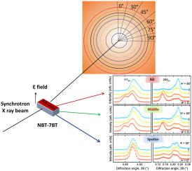
In situ, spatially-resolved synchrotron X-ray diffraction was utilized to investigate the electric field-induced heterogenous phase transformation of nonergodic relaxor 0.93Na1/2Bi1/2TiO3-0.07BaTiO3 ceramics. A Cu electrode was coated on one surface of a rectangular sample by aerosol deposition (AD), while a Pt layer was deposited on the opposite surface by sputter deposition. It is anticipated that a different stress state and/or domain morphology should occur on the AD deposited Cu electrode side due to the particle impact-consolidation deposition process. Under an electric field, different sample regions, i.e., AD, Middle, and Sputter sides, showed systematic changes in the relaxor to ferroelectric phase transition behavior. In particular, most <001> grains transformed at a sub-coercive field of 0.8 kV/mm, while the majority of the <111> grains only appeared to undergo transitions at a higher field (2.4 kV/mm). Also, the tetragonal phase became the dominant structure at higher field levels. Importantly, both <111> and <001> grains undergo phase switching at lower fields in the region close to the AD-processed layer. The study indicates that the AD process-induced stress can facilitate the electric field-induced relaxor to ferroelectric phase transition, i.e., the AD Cu side showed more significant lattice strain and domain texture than the sputter Pt side.
中文翻译:
0.93Na1/2Bi1/2TiO3-0.07BaTiO3 陶瓷中铁电相转换的空间分辨弛豫
利用空间分辨同步辐射X射线衍射原位研究了电场诱导的非过氧化弛豫0.93Na 1/2 Bi 1/2 TiO 3 -0.07BaTiO 3陶瓷的异相相变。通过气溶胶沉积 (AD) 将 Cu 电极涂覆在矩形样品的一个表面上,而通过溅射沉积将 Pt 层沉积在相对表面上。由于粒子冲击-固结沉积过程,预计在 AD 沉积的 Cu 电极侧应出现不同的应力状态和/或域形态。在一个电场下,不同的样本区域,即AD、中间和溅射面显示弛豫到铁电相变行为的系统变化。特别是,大多数 <001> 晶粒在 0.8 kV/mm 的亚矫顽力场下转变,而大多数 <111> 晶粒似乎只在更高的场 (2.4 kV/mm) 下经历转变。此外,四方相成为较高场级的主要结构。重要的是,<111> 和 <001> 晶粒都在靠近 AD 处理层的区域中的低场发生相转换。研究表明,AD工艺引起的应力可以促进电场引起的弛豫向铁电相转变,即AD Cu侧比溅射Pt侧表现出更显着的晶格应变和畴结构。


 京公网安备 11010802027423号