Applied Surface Science ( IF 6.7 ) Pub Date : 2022-01-15 , DOI: 10.1016/j.apsusc.2022.152499 Chandralina Patra 1 , Debajyoti Das 1
|
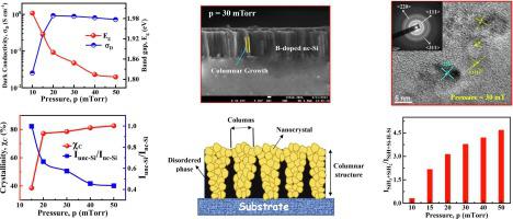
Boron-doped nc-Si thin films were developed on inexpensive, optically-transparent, and flexible PET-substrates at ambient-temperature (∼30 °C) using (SiH4 + B2H6)-plasma, without additional H2-dilution, by optimizing the gas pressure in inductively-coupled low-pressure plasma-CVD. An amorphous and monohydride-Si dominated partially-nanocrystalline network was obtained at pressure, p ≤ 15 mTorr. At higher pressure, the local plasma heating on the polymer-substrate by the high-density plasma-precursors and over-abundant atomic-H causes plasma-induced nano-bends, which trigger the stress-induced-crystallization of the network on the flexible substrate even at ambient-temperature. Although, the enhanced atomic-H reactivity on the growing-surface at very-high pressures causes the formation of the polyhydride-dominated defective grain-boundary, which acts as the electron-trapping-center and eventually reduces the dark-conductivity. At an optimum pressure of ∼30 mTorr, the transport of ample SiH3-radicals and atomic-H from the plasma appears instrumental in producing the p-nc-Si thin film with high-crystallinity (∼77%) in columnar-like growth morphology and adequately wide optical bandgap (∼1.88 eV). Substitution of the Si-atoms, primarily residing in the lattice within the core of Si-nanocrystals, by the electrically-active four-fold-coordinated B-atoms () generates high-density of free charge-carriers and contributes to high electrical-conductivity (∼1 S cm−1) of the room-temperature grown p-nc-Si thin film on the flexible PET-substrate, which seems suitable for the fabrication of low-cost flexible-electronics, including Si solar-cells.
中文翻译:
ICP-CVD在柔性聚合物基板上室温合成高导电B掺杂纳米晶硅薄膜
硼掺杂的 nc-Si 薄膜是在环境温度 (~30 °C) 下使用 (SiH 4 + B 2 H 6 ) 等离子体在廉价、光学透明和柔性 PET 基板上开发的,无需额外的 H 2-稀释,通过优化感应耦合低压等离子体CVD中的气体压力。在压力 p ≤ 15 mTorr 下获得了无定形和一氢化物-Si 为主的部分纳米晶网络。在较高的压力下,高密度等离子体前体和过量的原子-H 对聚合物基板的局部等离子体加热会导致等离子体诱导的纳米弯曲,从而触发柔性网络上的应力诱导结晶基板即使在环境温度下。虽然,在非常高的压力下,生长表面上增强的原子-H反应性导致形成以多氢化物为主的缺陷晶界,该晶界充当电子俘获中心并最终降低暗电导率。在 ∼30 mTorr 的最佳压力下,大量 SiH 3的传输来自等离子体的-自由基和原子-H似乎有助于产生具有高结晶度(~77%)的柱状生长形态和足够宽的光学带隙(~1.88 eV)的p -nc-Si薄膜。用电活性四重配位的 B 原子取代主要存在于 Si 纳米晶体核心内的晶格中的 Si 原子() 产生高密度的自由电荷载流子,并有助于在柔性 PET 基板上室温生长的p -nc-Si 薄膜的高电导率 (~1 S cm -1 ) ,这似乎适用于制造低成本的柔性电子产品,包括硅太阳能电池。


 京公网安备 11010802027423号