当前位置:
X-MOL 学术
›
Adv. Funct. Mater.
›
论文详情
Our official English website, www.x-mol.net, welcomes your feedback! (Note: you will need to create a separate account there.)
Quasi-Single Crystalline Cuprous Oxide Wafers via Stress-Assisted Thermal Oxidation for Optoelectronic Devices
Advanced Functional Materials ( IF 19.0 ) Pub Date : 2021-12-22 , DOI: 10.1002/adfm.202110505 Meng Xiao 1, 2 , Pengbin Gui 1, 2 , Kailian Dong 1, 2 , Liangbin Xiong 3 , Jiwei Liang 1, 2 , Fang Yao 1, 2 , Wenjing Li 1 , Yongjie Liu 1, 2 , Jiashuai Li 1, 2 , Weijun Ke 1, 2 , Chen Tao 1, 2 , Guojia Fang 1, 2
Advanced Functional Materials ( IF 19.0 ) Pub Date : 2021-12-22 , DOI: 10.1002/adfm.202110505 Meng Xiao 1, 2 , Pengbin Gui 1, 2 , Kailian Dong 1, 2 , Liangbin Xiong 3 , Jiwei Liang 1, 2 , Fang Yao 1, 2 , Wenjing Li 1 , Yongjie Liu 1, 2 , Jiashuai Li 1, 2 , Weijun Ke 1, 2 , Chen Tao 1, 2 , Guojia Fang 1, 2
Affiliation
|
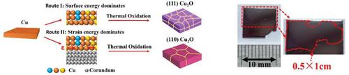
P-type semiconductor cuprous oxide (Cu2O) offers promising optoelectronic applications such as solar cells and photodetectors owing to its considerable absorption coefficients and high carrier mobility. However, polycrystalline Cu2O films with low carrier mobility resulting from excessive grain boundaries and structure disorder fail to meet the demands for these optoelectronic applications. Here a stress-assisted thermal oxidation method to fabricate p-type <110>-textured quasi-single crystalline Cu2O (c-Cu2O) wafers with centimeter-scale grains is developed. It is found that strain energy induced by thermal contact stress plays a critical role in crystal growth. The resultant <110>-textured quasi-single c-Cu2O wafers exhibit excellent crystallinity with rocking curve having a low full width at half maximum of 0.022°, a low defect density of 2 × 1011 cm−3, a high mobility exceeding 100 cm2 V−1 s−1, and a long minority lifetime of 98.5 µs. Such quasi-single c-Cu2O wafers lead to efficient solar cells with an open-circuit voltage of 0.95 V and highly responsive photodetectors with superior cycling stability. These results indicate not only the advancement of fabricating high-quality Cu2O wafers upon controllable methodology but also the promising optoelectronic applications using p-type metal oxide semiconductors.
中文翻译:

用于光电器件的应力辅助热氧化准单晶氧化亚铜晶片
P型半导体氧化亚铜(Cu 2 O)由于其可观的吸收系数和高载流子迁移率而提供了有前途的光电应用,例如太阳能电池和光电探测器。然而,由于过多的晶界和结构无序导致载流子迁移率低的多晶Cu 2 O薄膜无法满足这些光电应用的需求。这里采用应力辅助热氧化方法制备p型 <110> 织构准单晶 Cu 2 O (c-Cu 2O) 开发出具有厘米级晶粒的晶片。发现由热接触应力引起的应变能在晶体生长中起关键作用。所得<110>-织构准单c-Cu 2 O晶片表现出优异的结晶度,摇摆曲线具有0.022°的低半高宽、2×10 11 cm -3的低缺陷密度、高迁移率超过100 cm 2 V -1 s -1和98.5 µs的长少数寿命。这种准单c-Cu 2O 晶片可产生开路电压为 0.95 V 的高效太阳能电池和具有出色循环稳定性的高响应光电探测器。这些结果不仅表明了在可控方法上制造高质量 Cu 2 O 晶片的进步,而且表明了使用p型金属氧化物半导体的有前途的光电应用。
更新日期:2021-12-22
中文翻译:
用于光电器件的应力辅助热氧化准单晶氧化亚铜晶片
P型半导体氧化亚铜(Cu 2 O)由于其可观的吸收系数和高载流子迁移率而提供了有前途的光电应用,例如太阳能电池和光电探测器。然而,由于过多的晶界和结构无序导致载流子迁移率低的多晶Cu 2 O薄膜无法满足这些光电应用的需求。这里采用应力辅助热氧化方法制备p型 <110> 织构准单晶 Cu 2 O (c-Cu 2O) 开发出具有厘米级晶粒的晶片。发现由热接触应力引起的应变能在晶体生长中起关键作用。所得<110>-织构准单c-Cu 2 O晶片表现出优异的结晶度,摇摆曲线具有0.022°的低半高宽、2×10 11 cm -3的低缺陷密度、高迁移率超过100 cm 2 V -1 s -1和98.5 µs的长少数寿命。这种准单c-Cu 2O 晶片可产生开路电压为 0.95 V 的高效太阳能电池和具有出色循环稳定性的高响应光电探测器。这些结果不仅表明了在可控方法上制造高质量 Cu 2 O 晶片的进步,而且表明了使用p型金属氧化物半导体的有前途的光电应用。


 京公网安备 11010802027423号