Our official English website, www.x-mol.net, welcomes your feedback! (Note: you will need to create a separate account there.)
Direct Visualization and Manipulation of Tunable Quantum Well State in Semiconducting Nb2SiTe4
ACS Nano ( IF 17.1 ) Pub Date : 2021-10-13 , DOI: 10.1021/acsnano.1c03666 Jing Zhang 1, 2 , Zhilong Yang 3 , Shuai Liu 1, 2, 4 , Wei Xia 1, 5 , Tongshuai Zhu 3 , Cheng Chen 1, 6 , Chengwei Wang 1, 2, 7 , Meixiao Wang 1, 5 , Sung-Kwan Mo 6 , Lexian Yang 8 , Xufeng Kou 5, 9 , Yanfeng Guo 1 , Haijun Zhang 3 , Zhongkai Liu 1, 5 , Yulin Chen 1, 5, 8, 10
ACS Nano ( IF 17.1 ) Pub Date : 2021-10-13 , DOI: 10.1021/acsnano.1c03666 Jing Zhang 1, 2 , Zhilong Yang 3 , Shuai Liu 1, 2, 4 , Wei Xia 1, 5 , Tongshuai Zhu 3 , Cheng Chen 1, 6 , Chengwei Wang 1, 2, 7 , Meixiao Wang 1, 5 , Sung-Kwan Mo 6 , Lexian Yang 8 , Xufeng Kou 5, 9 , Yanfeng Guo 1 , Haijun Zhang 3 , Zhongkai Liu 1, 5 , Yulin Chen 1, 5, 8, 10
Affiliation
|
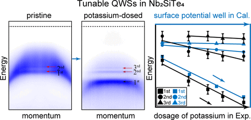
Quantum well states (QWSs) can form at the surface or interfaces of materials with confinement potential. They have broad applications in electronic and optical devices such as high mobility electron transistor, photodetector, and quantum well laser. The properties of the QWSs are usually the key factors for the performance of the devices. However, direct visualization and manipulation of such states are, in general, challenging. In this work, by using angle-resolved photoemission spectroscopy (ARPES) and scanning tunneling microscopy/spectroscopy (STM/STS), we directly probe the QWSs generated on the vacuum interface of a narrow band gap semiconductor Nb2SiTe4. Interestingly, the position and splitting of QWSs could be easily manipulated via potassium (K) dosage onto the sample surface. Our results suggest Nb2SiTe4 to be an intriguing semiconductor system to study and engineer the QWSs, which has great potential in device applications.
中文翻译:

半导体 Nb2SiTe4 中可调谐量子阱态的直接可视化和操纵
量子阱态 (QWS) 可以在具有限制势的材料的表面或界面处形成。它们在电子和光学器件中具有广泛的应用,例如高迁移率电子晶体管、光电探测器和量子阱激光器。QWS 的特性通常是影响器件性能的关键因素。然而,这些状态的直接可视化和操纵通常具有挑战性。在这项工作中,我们通过使用角分辨光电子能谱 (ARPES) 和扫描隧道显微镜/光谱学 (STM/STS),直接探测在窄带隙半导体 Nb 2 SiTe 4的真空界面上产生的QWS。. 有趣的是,QWS 的位置和分裂可以通过钾 (K) 剂量轻松控制到样品表面。我们的结果表明,Nb 2 SiTe 4是一种有趣的半导体系统,可以研究和设计 QWS,在器件应用中具有巨大潜力。
更新日期:2021-10-26
中文翻译:
半导体 Nb2SiTe4 中可调谐量子阱态的直接可视化和操纵
量子阱态 (QWS) 可以在具有限制势的材料的表面或界面处形成。它们在电子和光学器件中具有广泛的应用,例如高迁移率电子晶体管、光电探测器和量子阱激光器。QWS 的特性通常是影响器件性能的关键因素。然而,这些状态的直接可视化和操纵通常具有挑战性。在这项工作中,我们通过使用角分辨光电子能谱 (ARPES) 和扫描隧道显微镜/光谱学 (STM/STS),直接探测在窄带隙半导体 Nb 2 SiTe 4的真空界面上产生的QWS。. 有趣的是,QWS 的位置和分裂可以通过钾 (K) 剂量轻松控制到样品表面。我们的结果表明,Nb 2 SiTe 4是一种有趣的半导体系统,可以研究和设计 QWS,在器件应用中具有巨大潜力。


 京公网安备 11010802027423号