Our official English website, www.x-mol.net, welcomes your feedback! (Note: you will need to create a separate account there.)
Introducing Water Electrolithography
ACS Omega ( IF 4.1 ) Pub Date : 2021-09-21 , DOI: 10.1021/acsomega.1c03858 Sumit Kumar 1 , Ebinesh Abraham 1 , Praveen Kumar 2 , Rudra Pratap 1
ACS Omega ( IF 4.1 ) Pub Date : 2021-09-21 , DOI: 10.1021/acsomega.1c03858 Sumit Kumar 1 , Ebinesh Abraham 1 , Praveen Kumar 2 , Rudra Pratap 1
Affiliation
|
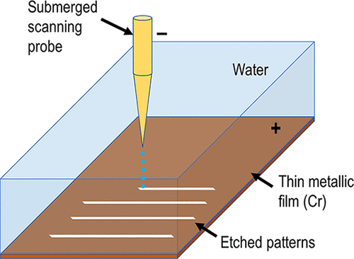
High-resolution patterning with remarkable customizability has stimulated the invention of numerous scanning probe lithography (SPL) techniques. However, frequent tip damage, substrate-film deterioration, low throughput, and debris amassing in the patterned region are the inherent impediments that have precluded obtaining patterns with high repeatability using SPL. Hence, SPL still has not got wider acceptance for industrial fabrication and technological applications. Here, we introduce a novel SPL technique, named water electrolithography (W-ELG), for patterning at the microscale and potentially at the nanoscale also. The technique operates in the non-contact mode and is based on the selective etching, via an electrochemical process, of a metallic film (e.g., Cr) submerged into water. Here, the working of W-ELG is demonstrated by scribing a pattern into the Cr film by a traversing cathode tip along a preset locus. A numerical analysis establishing the working principles and optimization strategies of W-ELG is also presented. The tip-sample distance and tip-diameter are identified as the critical parameters controlling the pattern creation. W-ELG achieved a throughput of 1.5 × 107 μm2/h, which is the highest among the existing SPL techniques, while drawing 4 μm wide lines, and is also immune to deleterious issues of tip damage, debris amassment, etc. Therefore, the resolution of these inherent impediments of SPL in W-ELG sets the stage for a paradigm shift that may now translate the SPL from academic exploration to industrial fabrications.
中文翻译:

介绍水电光刻
具有显着可定制性的高分辨率图案刺激了众多扫描探针光刻 (SPL) 技术的发明。然而,频繁的尖端损坏、基板薄膜退化、低吞吐量和图案区域中的碎片堆积是阻止使用 SPL 获得具有高重复性的图案的固有障碍。因此,SPL 在工业制造和技术应用方面仍未得到更广泛的认可。在这里,我们介绍了一种名为水电光刻 (W-ELG) 的新型 SPL 技术,用于在微米尺度上进行图案化,也可能在纳米尺度上进行图案化。该技术以非接触模式运行,并基于通过电化学过程对浸入水中的金属膜(例如,Cr)进行选择性蚀刻。这里,W-ELG 的工作原理是通过沿预设轨迹横穿阴极尖端在 Cr 膜中刻出图案来证明的。还介绍了建立 W-ELG 工作原理和优化策略的数值分析。针尖样本距离和针尖直径被确定为控制图案创建的关键参数。W-ELG 实现了 1.5 × 10 的吞吐量7 μm 2 /h 是现有 SPL 技术中最高的,同时绘制 4 μm 宽的线条,并且还不受尖端损坏、碎片堆积等有害问题的影响。因此,解决 SPL 的这些固有障碍W-ELG 为范式转变奠定了基础,现在可以将 SPL 从学术探索转化为工业制造。
更新日期:2021-10-06
中文翻译:
介绍水电光刻
具有显着可定制性的高分辨率图案刺激了众多扫描探针光刻 (SPL) 技术的发明。然而,频繁的尖端损坏、基板薄膜退化、低吞吐量和图案区域中的碎片堆积是阻止使用 SPL 获得具有高重复性的图案的固有障碍。因此,SPL 在工业制造和技术应用方面仍未得到更广泛的认可。在这里,我们介绍了一种名为水电光刻 (W-ELG) 的新型 SPL 技术,用于在微米尺度上进行图案化,也可能在纳米尺度上进行图案化。该技术以非接触模式运行,并基于通过电化学过程对浸入水中的金属膜(例如,Cr)进行选择性蚀刻。这里,W-ELG 的工作原理是通过沿预设轨迹横穿阴极尖端在 Cr 膜中刻出图案来证明的。还介绍了建立 W-ELG 工作原理和优化策略的数值分析。针尖样本距离和针尖直径被确定为控制图案创建的关键参数。W-ELG 实现了 1.5 × 10 的吞吐量7 μm 2 /h 是现有 SPL 技术中最高的,同时绘制 4 μm 宽的线条,并且还不受尖端损坏、碎片堆积等有害问题的影响。因此,解决 SPL 的这些固有障碍W-ELG 为范式转变奠定了基础,现在可以将 SPL 从学术探索转化为工业制造。


 京公网安备 11010802027423号