当前位置:
X-MOL 学术
›
Adv. Mater.
›
论文详情
Our official English website, www.x-mol.net, welcomes your feedback! (Note: you will need to create a separate account there.)
Heterogeneous Functional Dielectric Patterns for Charge-Carrier Modulation in Ultraflexible Organic Integrated Circuits
Advanced Materials ( IF 29.4 ) Pub Date : 2021-09-21 , DOI: 10.1002/adma.202104446 Koki Taguchi 1, 2, 3 , Takafumi Uemura 1, 2 , Naoko Namba 1, 2 , Andreas Petritz 4 , Teppei Araki 1, 2, 3 , Masahiro Sugiyama 1, 2, 3 , Barbara Stadlober 4 , Tsuyoshi Sekitani 1, 2, 3
Advanced Materials ( IF 29.4 ) Pub Date : 2021-09-21 , DOI: 10.1002/adma.202104446 Koki Taguchi 1, 2, 3 , Takafumi Uemura 1, 2 , Naoko Namba 1, 2 , Andreas Petritz 4 , Teppei Araki 1, 2, 3 , Masahiro Sugiyama 1, 2, 3 , Barbara Stadlober 4 , Tsuyoshi Sekitani 1, 2, 3
Affiliation
|
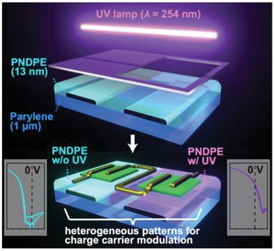
Flexible electronics have gained considerable attention for application in wearable devices. Organic transistors are potential candidates to develop flexible integrated circuits (ICs). A primary technique for maximizing their reliability, gain, and operation speed is the modulation of charge-carrier behavior in the respective transistors fabricated on the same substrate. In this work, heterogeneous functional dielectric patterns (HFDP) of ultrathin polymer gate dielectrics of poly((±)endo,exo-bicyclo[2.2.1]hept-ene-2,3-dicarboxylic acid, diphenylester) (PNDPE) are introduced. The HFDP that are obtained via the photo-Fries rearrangement by ultraviolet radiation in the homogeneous PNDPE provide a functional area for charge-carrier modulation. This leads to programmable threshold voltage control over a wide range (−1.5 to +0.2 V) in the transistors with a high patterning resolution, at 2 V operational voltage. The transistors also exhibit high operational stability over 140 days and under the bias-stress duration of 1800 s. With the HFDP, the performance metrics of ICs, for example, the noise margin and gain of the zero-VGS load inverters and the oscillation frequency of ring oscillators are improved to 80%, 1200, and 2.5 kHz, respectively, which are the highest among the previously reported zero-VGS-based organic circuits. The HFDP can be applied to much complex and ultraflexible ICs.
中文翻译:

用于超柔性有机集成电路中载流子调制的异质功能介电图案
柔性电子产品在可穿戴设备中的应用受到了广泛关注。有机晶体管是开发柔性集成电路 (IC) 的潜在候选者。最大化其可靠性、增益和操作速度的主要技术是调制在同一衬底上制造的各个晶体管中的电荷载流子行为。在这项工作中,介绍了聚((±)内,外-双环[2.2.1]庚烯-2,3-二羧酸,二苯酯)(PNDPE)的超薄聚合物栅极电介质的异质功能电介质图案(HFDP) . 在均质 PNDPE 中通过紫外线辐射通过 photo-Fries 重排获得的 HFDP 提供了一个用于电荷载流子调制的功能区域。这导致在宽范围(-1.5 至 +0. 2 V) 在具有高图案分辨率的晶体管中,工作电压为 2 V。在 140 天和 1800 秒的偏置应力持续时间下,晶体管还表现出很高的操作稳定性。使用 HFDP,IC 的性能指标,例如,零噪声容限和增益V GS负载逆变器和环形振荡器的振荡频率分别提高到 80%、1200 和 2.5 kHz,这是之前报道的基于零V GS的有机电路中最高的。HFDP 可以应用于许多复杂和超灵活的 IC。
更新日期:2021-11-09
中文翻译:
用于超柔性有机集成电路中载流子调制的异质功能介电图案
柔性电子产品在可穿戴设备中的应用受到了广泛关注。有机晶体管是开发柔性集成电路 (IC) 的潜在候选者。最大化其可靠性、增益和操作速度的主要技术是调制在同一衬底上制造的各个晶体管中的电荷载流子行为。在这项工作中,介绍了聚((±)内,外-双环[2.2.1]庚烯-2,3-二羧酸,二苯酯)(PNDPE)的超薄聚合物栅极电介质的异质功能电介质图案(HFDP) . 在均质 PNDPE 中通过紫外线辐射通过 photo-Fries 重排获得的 HFDP 提供了一个用于电荷载流子调制的功能区域。这导致在宽范围(-1.5 至 +0. 2 V) 在具有高图案分辨率的晶体管中,工作电压为 2 V。在 140 天和 1800 秒的偏置应力持续时间下,晶体管还表现出很高的操作稳定性。使用 HFDP,IC 的性能指标,例如,零噪声容限和增益V GS负载逆变器和环形振荡器的振荡频率分别提高到 80%、1200 和 2.5 kHz,这是之前报道的基于零V GS的有机电路中最高的。HFDP 可以应用于许多复杂和超灵活的 IC。


 京公网安备 11010802027423号