当前位置:
X-MOL 学术
›
Small Methods
›
论文详情
Our official English website, www.x-mol.net, welcomes your feedback! (Note: you will need to create a separate account there.)
Large-Area MoS2 via Colloidal Nanosheet Ink for Integrated Memtransistor
Small Methods ( IF 12.4 ) Pub Date : 2021-09-17 , DOI: 10.1002/smtd.202100558 Duc Anh Nguyen 1 , Dae Young Park 2 , Ngoc Thanh Duong 3 , Kang-Nyeoung Lee 4 , Hyunsik Im 1 , Heejun Yang 5 , Mun Seok Jeong 2
Small Methods ( IF 12.4 ) Pub Date : 2021-09-17 , DOI: 10.1002/smtd.202100558 Duc Anh Nguyen 1 , Dae Young Park 2 , Ngoc Thanh Duong 3 , Kang-Nyeoung Lee 4 , Hyunsik Im 1 , Heejun Yang 5 , Mun Seok Jeong 2
Affiliation
|
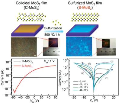
2D transition metal dichalcogenides (TMDs) exhibit intriguing properties for applications in optoelectronics and electronics, among which memtransistors received extensive attention as multifunctional devices. For practical applications of 2D TMDs, large-area fabrication of the materials via reliable processes, which is in trade-off with their quality, has been a long-standing issue. Here, a simple and effective way is proposed to fabricate large-area and high-quality molybdenum disulfide thin films using MoS2 colloidal ink through a spray coating, followed by a postsulfurization process. High-quality MoS2 thin films exhibit excellent optical and electrical properties that can be utilized in field-effect transistors (FETs) and memtransistor arrays. The MoS2 FETs show an average on/off ratio of 5 × 10⁶ and a high electron mobility of 10.34 cm2 V−1 s−1, which can be understood by the healing of sulfur vacancies, recrystallization, and the removal of the carbon contamination of the MoS2. These MoS2-based memtransistors present stable operations with a high switching ratio tuned by back gate and light illumination, which is promising for multiple-levels memory and complex neuromorphic computing. This study demonstrates a new strategy to fabricate 2D TMDs with large-area and high quality for integrated optoelectronic and memory device applications.
中文翻译:

大面积二硫化钼通过胶体纳米片墨水用于集成忆阻器
二维过渡金属二硫属化物 (TMD) 在光电子学和电子学中的应用中表现出有趣的特性,其中记忆晶体管作为多功能器件受到广泛关注。对于二维 TMD 的实际应用,通过可靠的工艺大面积制造材料,这与其质量进行权衡,一直是一个长期存在的问题。在这里,提出了一种简单有效的方法,通过喷涂,然后进行后硫化工艺,使用 MoS 2胶体油墨制备大面积和高质量的二硫化钼薄膜。高质量的 MoS 2薄膜表现出优异的光学和电学特性,可用于场效应晶体管 (FET) 和记忆晶体管阵列。MoS 2FET 显示出 5 × 10 6的平均开/关比和 10.34 cm 2 V -1 s -1的高电子迁移率,这可以通过硫空位的愈合、重结晶和去除碳污染来理解MoS 2。这些基于MoS 2的记忆晶体管表现出稳定的操作,具有通过背栅和光照明调节的高开关比,这对于多级记忆和复杂的神经形态计算很有前景。这项研究展示了一种新策略,可以为集成光电和存储器件应用制造大面积、高质量的 2D TMD。
更新日期:2021-11-12
中文翻译:
大面积二硫化钼通过胶体纳米片墨水用于集成忆阻器
二维过渡金属二硫属化物 (TMD) 在光电子学和电子学中的应用中表现出有趣的特性,其中记忆晶体管作为多功能器件受到广泛关注。对于二维 TMD 的实际应用,通过可靠的工艺大面积制造材料,这与其质量进行权衡,一直是一个长期存在的问题。在这里,提出了一种简单有效的方法,通过喷涂,然后进行后硫化工艺,使用 MoS 2胶体油墨制备大面积和高质量的二硫化钼薄膜。高质量的 MoS 2薄膜表现出优异的光学和电学特性,可用于场效应晶体管 (FET) 和记忆晶体管阵列。MoS 2FET 显示出 5 × 10 6的平均开/关比和 10.34 cm 2 V -1 s -1的高电子迁移率,这可以通过硫空位的愈合、重结晶和去除碳污染来理解MoS 2。这些基于MoS 2的记忆晶体管表现出稳定的操作,具有通过背栅和光照明调节的高开关比,这对于多级记忆和复杂的神经形态计算很有前景。这项研究展示了一种新策略,可以为集成光电和存储器件应用制造大面积、高质量的 2D TMD。


 京公网安备 11010802027423号