Surfaces and Interfaces ( IF 6.2 ) Pub Date : 2021-09-15 , DOI: 10.1016/j.surfin.2021.101457 Avinash C. Mendhe 1 , Sutripto Majumder 2 , Sambhaji M. Pawar 3 , Babasaheb R. Sankapal 1
|
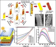
Present research explores the first report for encapsulation of Bi2S3 nanoparticles (NPs) on the surface of the chemical bath deposited one dimensional CdS nanowires (NWs) enabling core-shell surface architecture with the aid of simple and low-cost successive ionic layer adsorption and reaction (SILAR) method towards photo electrochemical solar cell application. Optimum coverage of well-tuned Bi2S3 particle size on CdS NWs through number of SILAR immersions implicit nano heterostructure at core-shell interfacial contact as examined through structural, surface morphological, and valence state elemental analysis in correlation with the photoelectrochemical (PEC) solar cell parameters as efficiency, quantum efficiency, Mott-Schottky and electrochemical resistances along with electron lifetime through EIS studies. Remarkably, 15 SILAR cycled Bi2S3 anchored CdS NWs yields one and half times better efficiency than the bare CdS and three times than bare Bi2S3. Incorporation of lower band gap material over the larger band gap semiconductor with well-tuned particle size and energy band alignment has opened an auspicious route to enhance the light harvesting property as explored through CdS NWs/ Bi2S3 nano heterostructure.
中文翻译:
CdS 纳米线表面的 Bi2S3 纳米颗粒:面向太阳能电池应用的核壳纳米结构设计
目前的研究探索了第一份关于在化学浴表面上封装 Bi 2 S 3纳米粒子 (NPs) 的报告,该化学浴沉积了一维 CdS 纳米线 (NWs),借助简单且低成本的连续离子层实现核壳表面结构用于光电化学太阳能电池应用的吸附和反应(SILAR)方法。优化好的 Bi 2 S 3覆盖范围通过与光电化学 (PEC) 太阳能电池参数(如效率、量子效率、莫特)相关的结构、表面形态和价态元素分析,通过 SILAR 浸入次数确定 CdS NW 上的粒径- 肖特基电阻和电化学电阻以及通过 EIS 研究的电子寿命。值得注意的是,15 个 SILAR 循环的 Bi 2 S 3锚定 CdS NW 的效率是裸 CdS 的一倍半,是裸 Bi 2 S 3 的三倍. 如通过 CdS NWs/Bi 2 S 3纳米异质结构探索的那样,在较大带隙半导体上并入具有良好调谐的粒径和能带排列的较低带隙材料开辟了增强光收集特性的有利途径。


 京公网安备 11010802027423号