当前位置:
X-MOL 学术
›
Adv. Funct. Mater.
›
论文详情
Our official English website, www.x-mol.net, welcomes your feedback! (Note: you will need to create a separate account there.)
Self-Assembled Perovskite Nanoislands on CH3NH3PbI3 Cuboid Single Crystals by Energetic Surface Engineering
Advanced Functional Materials ( IF 19.0 ) Pub Date : 2021-09-12 , DOI: 10.1002/adfm.202105542 Yurou Zhang 1 , Dohyung Kim 2, 3 , Jung‐Ho Yun 1 , Jongchul Lim 4, 5 , Min‐Cherl Jung 6 , Xiaoming Wen 7 , Jan Seidel 3 , Eunyoung Choi 8 , Mu Xiao 1 , Tengfei Qiu 1 , Miaoqiang Lyu 1 , EQ Han 1 , Mehri Ghasemi 7 , Sean Lim 9 , Henry J. Snaith 4 , Jae Sung Yun 8 , Lianzhou Wang 1
Advanced Functional Materials ( IF 19.0 ) Pub Date : 2021-09-12 , DOI: 10.1002/adfm.202105542 Yurou Zhang 1 , Dohyung Kim 2, 3 , Jung‐Ho Yun 1 , Jongchul Lim 4, 5 , Min‐Cherl Jung 6 , Xiaoming Wen 7 , Jan Seidel 3 , Eunyoung Choi 8 , Mu Xiao 1 , Tengfei Qiu 1 , Miaoqiang Lyu 1 , EQ Han 1 , Mehri Ghasemi 7 , Sean Lim 9 , Henry J. Snaith 4 , Jae Sung Yun 8 , Lianzhou Wang 1
Affiliation
|
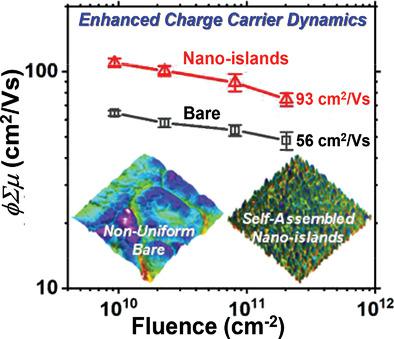
Organometal perovskite single crystals have been recognized as a promising platform for high-performance optoelectronic devices, featuring high crystallinity and stability. However, a high trap density and structural nonuniformity at the surface have been major barriers to the progress of single crystal-based optoelectronic devices. Here, the formation of a unique nanoisland structure is reported at the surface of the facet-controlled cuboid MAPbI3 (MA = CH3NH3+) single crystals through a cation interdiffusion process enabled by energetically vaporized CsI. The interdiffusion of mobile ions between the bulk and the surface is triggered by thermally activated CsI vapor, which reconstructs the surface that is rich in MA and CsI with reduced dangling bonds. Simultaneously, an array of Cs-Pb-rich nanoislands is constructed on the surface of the MAPbI3 single crystals. This newly reconstructed nanoisland surface enhances the light absorbance over 50% and increases the charge carrier mobility from 56 to 93 cm2 V−1 s−1. As confirmed by Kelvin probe force microscopy, the nanoislands form a gradient band bending that prevents recombination of excess carriers, and thus, enhances lateral carrier transport properties. This unique engineering of the single crystal surface provides a pathway towards developing high-quality perovskite single-crystal surface for optoelectronic applications.
中文翻译:

通过高能表面工程在 CH3NH3PbI3 长方体单晶上自组装钙钛矿纳米岛
有机金属钙钛矿单晶已被公认为高性能光电器件的有前途的平台,具有高结晶度和稳定性。然而,表面的高陷阱密度和结构不均匀性一直是单晶光电器件发展的主要障碍。在这里,在小平面控制的长方体 MAPbI 3 (MA = CH 3 NH 3 +) 单晶通过由能量蒸发的 CsI 实现的阳离子相互扩散过程。主体和表面之间的移动离子的相互扩散是由热激活的 CsI 蒸气触发的,它重建了富含 MA 和 CsI 的表面,并具有减少的悬空键。同时,在 MAPbI 3单晶表面构建了一系列富含 Cs-Pb 的纳米岛。这种新重建的纳米岛表面将光吸收率提高了 50% 以上,并将电荷载流子迁移率从 56 增加到 93 cm 2 V -1 s -1. 开尔文探针力显微镜证实,纳米岛形成梯度带弯曲,防止多余载流子的重组,从而增强横向载流子传输特性。这种独特的单晶表面工程为开发用于光电应用的高质量钙钛矿单晶表面提供了途径。
更新日期:2021-09-12
中文翻译:
通过高能表面工程在 CH3NH3PbI3 长方体单晶上自组装钙钛矿纳米岛
有机金属钙钛矿单晶已被公认为高性能光电器件的有前途的平台,具有高结晶度和稳定性。然而,表面的高陷阱密度和结构不均匀性一直是单晶光电器件发展的主要障碍。在这里,在小平面控制的长方体 MAPbI 3 (MA = CH 3 NH 3 +) 单晶通过由能量蒸发的 CsI 实现的阳离子相互扩散过程。主体和表面之间的移动离子的相互扩散是由热激活的 CsI 蒸气触发的,它重建了富含 MA 和 CsI 的表面,并具有减少的悬空键。同时,在 MAPbI 3单晶表面构建了一系列富含 Cs-Pb 的纳米岛。这种新重建的纳米岛表面将光吸收率提高了 50% 以上,并将电荷载流子迁移率从 56 增加到 93 cm 2 V -1 s -1. 开尔文探针力显微镜证实,纳米岛形成梯度带弯曲,防止多余载流子的重组,从而增强横向载流子传输特性。这种独特的单晶表面工程为开发用于光电应用的高质量钙钛矿单晶表面提供了途径。


 京公网安备 11010802027423号