当前位置:
X-MOL 学术
›
Phys. Rev. Materials
›
论文详情
Our official English website, www.x-mol.net, welcomes your feedback! (Note: you will need to create a separate account there.)
Direct band gap halide-double-perovskite absorbers for solar cells and light emitting diodes:Ab initiostudy of bulk and layers
Physical Review Materials ( IF 3.4 ) Pub Date : 2021-09-09 , DOI: 10.1103/physrevmaterials.5.095401 Anu Bala 1 , Vijay Kumar 1, 2
Physical Review Materials ( IF 3.4 ) Pub Date : 2021-09-09 , DOI: 10.1103/physrevmaterials.5.095401 Anu Bala 1 , Vijay Kumar 1, 2
Affiliation
|
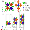
We present results of a state-of-the-art computational study of the atomic and electronic structure of (, Ag; , Bi; , Br, I) layers with up to three-unit-cell thickness () as well as their bulk counterparts in the search for economical and stable halide double perovskites (HDPs) with a direct band gap and strong light absorption. Among the 24 layers we have studied, seven are found to be suitable for light emitting diodes, whereas one is proposed for solar cell applications. Our results on bulk (, Bi; , Br) HDPs agree with previous studies. Interestingly, we find that HDP layers as well as bulk are more stable than their respective lead-halide perovskites. The Cu-based HDPs are cost effective compared with those based on Ag and are found to be equally suitable as absorber materials with a lower band gap. However, bulk (, Br) HDPs are found to be dynamically unstable. Our calculations show a combined effect of confinement and spin-orbit coupling in deciding the nature of the band gap for one (two)-unit-cell thick layers of (). Furthermore, strong confinement effects are found to be crucial in making the thinnest layers of (, Br) direct band gap semiconductors. The reduction in the dimension from three to two dimensions introduces distortions in the layers of the HDPs, and it is more in the case of the Cu-based layers. The nature of the band gap becomes direct for very thin layers of () and (, 2) compared with indirect band gap in bulk. The HDP layers with a direct band gap and enhanced stability also have a strong absorption coefficient of the order of , making them interesting for solar cell applications. The effects of surfaces on the electronic structure of direct band gap layers of (, 2) and () are also shown with surface states. We hope that our results on HDPs will stimulate further research on these materials.
中文翻译:

用于太阳能电池和发光二极管的直接带隙卤化物-双钙钛矿吸收剂:体和层的初步研究
我们展示了原子和电子结构的最新计算研究结果 (,银; , 毕; , Br, I) 层的厚度高达三个单元电池 () 以及它们的本体对应物,以寻找具有直接带隙和强光吸收的经济且稳定的卤化物双钙钛矿 (HDP)。在我们研究的 24 层中,发现有 7 层适用于发光二极管,而有 1 层适用于太阳能电池应用。我们的批量结果 (, 毕; , Br) HDPs 与之前的研究一致。有趣的是,我们发现 HDP 层和块体比它们各自的卤化铅钙钛矿更稳定。与基于 Ag 的 HDP 相比,基于 Cu 的 HDP 具有成本效益,并且被发现同样适合作为具有较低带隙的吸收材料。然而,散装 (, Br) HDP 被发现是动态不稳定的。我们的计算显示了限制和自旋轨道耦合在决定一(两)个晶胞厚层的带隙性质方面的综合影响 ()。此外,发现强限制效应对于制造最薄的层是至关重要的。 (, Br) 直接带隙半导体。维度从三个维度减少到两个维度会在 HDP 的层中引入畸变,并且在基于 Cu 的层的情况下更是如此。对于非常薄的层,带隙的性质变得直接 () 和 (, 2) 与散装间接带隙相比。具有直接带隙和增强稳定性的 HDP 层也具有大约为,使它们对太阳能电池应用很有趣。表面对直接带隙层电子结构的影响 (, 2和 () 也显示了表面状态。我们希望我们在 HDP 上的结果将刺激对这些材料的进一步研究。
更新日期:2021-09-10
中文翻译:
用于太阳能电池和发光二极管的直接带隙卤化物-双钙钛矿吸收剂:体和层的初步研究
我们展示了原子和电子结构的最新计算研究结果 (,银; , 毕; , Br, I) 层的厚度高达三个单元电池 () 以及它们的本体对应物,以寻找具有直接带隙和强光吸收的经济且稳定的卤化物双钙钛矿 (HDP)。在我们研究的 24 层中,发现有 7 层适用于发光二极管,而有 1 层适用于太阳能电池应用。我们的批量结果 (, 毕; , Br) HDPs 与之前的研究一致。有趣的是,我们发现 HDP 层和块体比它们各自的卤化铅钙钛矿更稳定。与基于 Ag 的 HDP 相比,基于 Cu 的 HDP 具有成本效益,并且被发现同样适合作为具有较低带隙的吸收材料。然而,散装 (, Br) HDP 被发现是动态不稳定的。我们的计算显示了限制和自旋轨道耦合在决定一(两)个晶胞厚层的带隙性质方面的综合影响 ()。此外,发现强限制效应对于制造最薄的层是至关重要的。 (, Br) 直接带隙半导体。维度从三个维度减少到两个维度会在 HDP 的层中引入畸变,并且在基于 Cu 的层的情况下更是如此。对于非常薄的层,带隙的性质变得直接 () 和 (, 2) 与散装间接带隙相比。具有直接带隙和增强稳定性的 HDP 层也具有大约为,使它们对太阳能电池应用很有趣。表面对直接带隙层电子结构的影响 (, 2和 () 也显示了表面状态。我们希望我们在 HDP 上的结果将刺激对这些材料的进一步研究。


 京公网安备 11010802027423号