当前位置:
X-MOL 学术
›
ACS Appl. Electron. Mater.
›
论文详情
Our official English website, www.x-mol.net, welcomes your feedback! (Note: you will need to create a separate account there.)
High-Performance and Ultralow-Noise Two-Dimensional Heterostructure Field-Effect Transistors with One-Dimensional Electrical Contacts
ACS Applied Electronic Materials ( IF 4.7 ) Pub Date : 2021-09-07 , DOI: 10.1021/acsaelm.1c00595 Aroop K. Behera 1 , Charles Thomas Harris 2, 3 , Douglas V. Pete 2, 3 , Collin J. Delker 3 , Per Erik Vullum 4 , Marta B. Muniz 5, 6 , Ozhan Koybasi 7 , Takashi Taniguchi 8 , Kenji Watanabe 9 , Branson D. Belle 5 , Suprem R. Das 1, 10
ACS Applied Electronic Materials ( IF 4.7 ) Pub Date : 2021-09-07 , DOI: 10.1021/acsaelm.1c00595 Aroop K. Behera 1 , Charles Thomas Harris 2, 3 , Douglas V. Pete 2, 3 , Collin J. Delker 3 , Per Erik Vullum 4 , Marta B. Muniz 5, 6 , Ozhan Koybasi 7 , Takashi Taniguchi 8 , Kenji Watanabe 9 , Branson D. Belle 5 , Suprem R. Das 1, 10
Affiliation
|
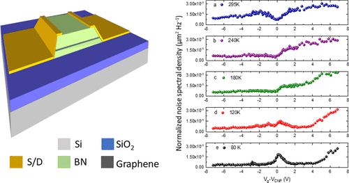
Two-dimensional heterostructure field-effect transistors (2D-HFETs) with one-dimensional electrical contacts to atomically thin channels have recently shown great device performance, such as reduced contact resistance, leading to ballistic transport and enhanced carrier mobility. While a number of low-frequency noise studies exists on bare graphene devices supported on silicon dioxide gate insulators with surface contacts, such studies in heterostructure devices comprising epitaxial graphene on hexagonal boron nitride (hBN) with edge contacts are extremely limited. In this article, we present a systematic, temperature-dependent study of electrical transport and low-frequency noise in edge-contacted high-mobility HFET with a single atomic-layer graphene channel encapsulated by hBN and demonstrate ultralow noise with a Hooge parameter of ≈10–5. By combining measurements and modeling based on underlying microscopic scattering mechanisms caused by charge carriers and phonons, we directly correlate the high-performance, temperature-dependent transport behavior of this device with the noise characteristics. Our study provides a pathway towards engineering low-noise graphene-based high-performance 2D-FETs with one-dimensional edge contacts for applications such as digital electronics and chemical/biological sensing.
中文翻译:

具有一维电触点的高性能和超低噪声二维异质结构场效应晶体管
二维异质结构场效应晶体管 (2D-HFET) 与原子级薄通道的一维电接触最近显示出良好的器件性能,例如降低接触电阻,导致弹道传输和增强的载流子迁移率。虽然在具有表面接触的二氧化硅栅极绝缘体上支撑的裸石墨烯器件上存在许多低频噪声研究,但在具有边缘接触的六方氮化硼 (hBN) 上包含外延石墨烯的异质结构器件中的此类研究极为有限。在本文中,我们对边缘接触的高迁移率 HFET 中的电传输和低频噪声进行了系统的、温度相关的研究,该 HFET 具有由 hBN 封装的单个原子层石墨烯通道,并展示了 Hooge 参数为 ≈ 的超低噪声10–5 . 通过结合基于由电荷载流子和声子引起的潜在微观散射机制的测量和建模,我们将该设备的高性能、温度相关传输行为与噪声特性直接相关。我们的研究为设计具有一维边缘接触的基于低噪声石墨烯的高性能 2D-FET 提供了一条途径,用于数字电子和化学/生物传感等应用。
更新日期:2021-09-28
中文翻译:
具有一维电触点的高性能和超低噪声二维异质结构场效应晶体管
二维异质结构场效应晶体管 (2D-HFET) 与原子级薄通道的一维电接触最近显示出良好的器件性能,例如降低接触电阻,导致弹道传输和增强的载流子迁移率。虽然在具有表面接触的二氧化硅栅极绝缘体上支撑的裸石墨烯器件上存在许多低频噪声研究,但在具有边缘接触的六方氮化硼 (hBN) 上包含外延石墨烯的异质结构器件中的此类研究极为有限。在本文中,我们对边缘接触的高迁移率 HFET 中的电传输和低频噪声进行了系统的、温度相关的研究,该 HFET 具有由 hBN 封装的单个原子层石墨烯通道,并展示了 Hooge 参数为 ≈ 的超低噪声10–5 . 通过结合基于由电荷载流子和声子引起的潜在微观散射机制的测量和建模,我们将该设备的高性能、温度相关传输行为与噪声特性直接相关。我们的研究为设计具有一维边缘接触的基于低噪声石墨烯的高性能 2D-FET 提供了一条途径,用于数字电子和化学/生物传感等应用。


 京公网安备 11010802027423号