当前位置:
X-MOL 学术
›
ACS Appl. Nano Mater.
›
论文详情
Our official English website, www.x-mol.net, welcomes your feedback! (Note: you will need to create a separate account there.)
Critical Behavior in Au Nanoparticle Arrays: Implications for All-Metal Field Effect Transistors with Ultra-high Gain at Room Temperature
ACS Applied Nano Materials ( IF 5.9 ) Pub Date : 2021-09-03 , DOI: 10.1021/acsanm.1c01641 Abhijeet Prasad 1 , Michael Stoller 2 , Ravi F. Saraf 1, 3
ACS Applied Nano Materials ( IF 5.9 ) Pub Date : 2021-09-03 , DOI: 10.1021/acsanm.1c01641 Abhijeet Prasad 1 , Michael Stoller 2 , Ravi F. Saraf 1, 3
Affiliation
|
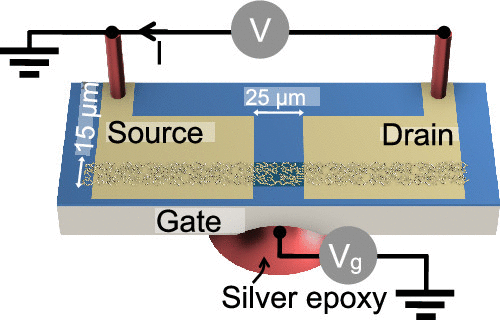
The working principle of large-area, open-gate field effect transistors (ogFETs) is attractive for the high-sensitivity detection of chemicals and interfacing with single cells. We describe an ogFET composed of a self-assembled, two-dimensional (2D) random network of 1D chains of 10 nm Au particles spanning over 25 μm. The device has a gating gain of 103-fold at room temperature (RT) compared to <50% for reported nanoparticle arrays at RT. The current, I ∼ (V – VT)ζ, is functionally identical to the Coulomb blockade (CB) effect observed at cryogenic temperatures, and the conductance gap, VT, at room temperature cannot be attributed to local charging for large particles (>5 nm). Surprisingly, unlike the effect observed in CB, the VT remains invariant over a large gating potential 0–25 V, leading to a universal behavior where all the I–V curves collapse into a single master curve. We explain the universality as a classical critical behavior by quantitatively mapping the percolation path in real-space images. The paths evolve as self-similar percolation channels in a fractal dimension of 1.88. The device principle enables a 103-fold gating gain in all-metallic nanoparticle arrays at RT and will potentially lead to ogFET sensors and electrochemical devices with liquid-gate junctions. The critical behavior with bias may serve as a model system to study the electronic transport in these exotic systems.
中文翻译:

金纳米粒子阵列的关键行为:对室温下具有超高增益的全金属场效应晶体管的影响
大面积开栅场效应晶体管 (ogFET) 的工作原理对于化学物质的高灵敏度检测和与单个电池的接口很有吸引力。我们描述了一个 ogFET,它由跨越 25 μm 的 10 nm Au 粒子的一维链的自组装二维 (2D) 随机网络组成。该装置在室温 (RT) 下具有 10 3倍的选通增益,而在 RT 下报道的纳米颗粒阵列的门控增益小于 50%。电流I ∼ ( V – V T ) ζ在功能上与在低温下观察到的库仑阻塞 (CB) 效应和电导间隙V T 相同, 在室温下不能归因于大颗粒 (> 5 nm) 的局部充电。令人惊讶的是,与在 CB 中观察到的效应不同,V T在 0-25 V 的大门控电位上保持不变,导致所有I - V曲线折叠成一条主曲线的普遍行为。我们通过定量映射真实空间图像中的渗透路径来将普遍性解释为经典的临界行为。路径演变为分形维数为 1.88 的自相似渗透通道。设备原理使 10 3全金属纳米粒子阵列在 RT 中的 - 倍门控增益,并可能导致 ogFET 传感器和具有液门结的电化学设备。带有偏差的临界行为可以作为研究这些奇异系统中电子传输的模型系统。
更新日期:2021-09-24
中文翻译:
金纳米粒子阵列的关键行为:对室温下具有超高增益的全金属场效应晶体管的影响
大面积开栅场效应晶体管 (ogFET) 的工作原理对于化学物质的高灵敏度检测和与单个电池的接口很有吸引力。我们描述了一个 ogFET,它由跨越 25 μm 的 10 nm Au 粒子的一维链的自组装二维 (2D) 随机网络组成。该装置在室温 (RT) 下具有 10 3倍的选通增益,而在 RT 下报道的纳米颗粒阵列的门控增益小于 50%。电流I ∼ ( V – V T ) ζ在功能上与在低温下观察到的库仑阻塞 (CB) 效应和电导间隙V T 相同, 在室温下不能归因于大颗粒 (> 5 nm) 的局部充电。令人惊讶的是,与在 CB 中观察到的效应不同,V T在 0-25 V 的大门控电位上保持不变,导致所有I - V曲线折叠成一条主曲线的普遍行为。我们通过定量映射真实空间图像中的渗透路径来将普遍性解释为经典的临界行为。路径演变为分形维数为 1.88 的自相似渗透通道。设备原理使 10 3全金属纳米粒子阵列在 RT 中的 - 倍门控增益,并可能导致 ogFET 传感器和具有液门结的电化学设备。带有偏差的临界行为可以作为研究这些奇异系统中电子传输的模型系统。


 京公网安备 11010802027423号