Journal of Electronic Materials ( IF 2.1 ) Pub Date : 2021-07-13 , DOI: 10.1007/s11664-021-09058-5 C. C. Ciobotaru 1 , I. C. Ciobotaru 1 , S. Polosan 1 , D. G. Iosub 2
|
Abstract
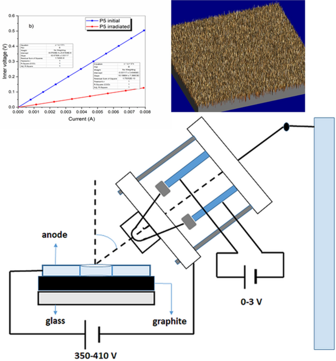
Highly conductive carbon-based thin films have been produced by low-energy electron irradiation. Low-energy electron irradiation at a lower density of electrons eliminates the sp3 hybridization of the carbon atoms by reducing the chemical groups on the surface. Irradiated carbon-based thin films became highly conductive layers that could be used as electrodes for optoelectronic devices. The electrical conductivity σ reached 3 × 10⁴ S/m in the case of samples irradiated at a lower density, with a mean value between 3 × 10⁵ S/m and 3.3 × 10² S/m for highly crystalline graphite structures. The increasing (002) peak diffraction and decreasing intensity ratio ID/IG in the Raman spectra as well as the decreasing bandgap in photoluminescence measurements demonstrated the reduction of oxygen-induced defects in these thin films.
Graphic Abstract
中文翻译:
低能电子辐照制备的高导电碳基薄膜
摘要
高导电碳基薄膜已通过低能电子辐射制备。低电子密度下的低能电子辐射通过减少表面上的化学基团来消除碳原子的sp 3杂化。辐照后的碳基薄膜成为高导电层,可用作光电器件的电极。 在较低密度照射的样品的情况下,电导率σ达到3×10 4 S/m, 对于高结晶石墨结构,其平均值在3×10 5 S/m和3.3×10 2 S/m之间。增加(002)峰衍射和减少强度比I D/我ģ拉曼光谱中,以及在光致发光测量的降低的带隙表现在这些薄膜的氧引起的缺陷的减少。


 京公网安备 11010802027423号