当前位置:
X-MOL 学术
›
Phys. Status Solidi B
›
论文详情
Our official English website, www.x-mol.net, welcomes your feedback! (Note: you will need to create a separate account there.)
Amorphous SiSn Alloy: Another Candidate Material for Temperature Sensing Layers in Uncooled Microbolometers
Physica Status Solidi (B) - Basic Solid State Physics ( IF 1.6 ) Pub Date : 2021-08-24 , DOI: 10.1002/pssb.202100103 Hazem ElGhonimy 1 , Mohamed Ramy Abdel-Rahman 1, 2 , Mahmoud Hezam 2 , Mohammad Alduraibi 2, 3 , Nageeb Al-Khalli 1 , Bouraoui Ilahi 4
Physica Status Solidi (B) - Basic Solid State Physics ( IF 1.6 ) Pub Date : 2021-08-24 , DOI: 10.1002/pssb.202100103 Hazem ElGhonimy 1 , Mohamed Ramy Abdel-Rahman 1, 2 , Mahmoud Hezam 2 , Mohammad Alduraibi 2, 3 , Nageeb Al-Khalli 1 , Bouraoui Ilahi 4
Affiliation
|
Herein, the prospect of using amorphous Si1–x
Sn
x
alloys as alternative temperature-sensing active materials in microbolometers is evaluated by studying their temperature-dependent resistive properties along with their infrared optical properties. Si1–x
Sn
x
thin films (200 nm thick), with varying Sn concentrations, are prepared at room temperature by cosputtering from Si and Sn targets using simultaneous radio frequency and DC magnetron sputter deposition. Low beam energy X-ray microanalysis is used to estimate the atomic concentrations of the prepared films. Atomic force microscopy analysis shows an increase in the root-mean-square surface roughness of the prepared Si1–x
Sn
x
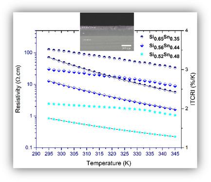
thin films, with increasing Sn content. Sheet resistance versus temperature measurements are performed yielding temperature coefficients of resistance of 3.25, 2.65, and 1.72% K−1 at resistivity values of 116.18, 27.36, and 2.34 Ω cm for Sn concentrations of 35%, 44%, and 48%, respectively. Infrared ellipsometry measurements are performed to extract the optical properties of the Si1–x
Sn
x
thin films and optical simulations confirm that a Fabry–Pérot cavity microbolometer configuration containing an Si1–x
Sn
x
thin film can achieve high absorptance in the 8–12 μm band. This study shows that Si1–x
Sn
x
alloys are a suitable, simple, and low-cost replacement for thermometer layers used in uncooled infrared microbolometers.
中文翻译:

非晶硅锡合金:另一种用于非冷却微测辐射热计温度传感层的候选材料
在此,通过研究非晶态 Si 1- x Sn x合金作为微测辐射热计中替代温度传感活性材料的前景,通过研究它们的温度相关电阻特性及其红外光学特性进行了评估。Si 1– x Sn x薄膜(200 nm 厚),具有不同的 Sn 浓度,在室温下通过使用同步射频和 DC 磁控管溅射沉积从 Si 和 Sn 靶材共溅射制备。低束能量 X 射线微量分析用于估计所制备薄膜的原子浓度。原子力显微镜分析表明制备的 Si 1– x的均方根表面粗糙度增加 Sn x薄膜,随着 Sn 含量的增加。进行薄层电阻与温度测量的结果分别在116.18、27.36 和 2.34 Ω cm 的电阻率值下对于 35%、44% 和 48% 的 Sn 浓度产生 3.25、2.65和 1.72% K -1的电阻温度系数. 进行红外椭偏测量以提取 Si 1– x Sn x薄膜的光学特性,光学模拟证实包含 Si 1– x Sn x薄膜的法布里-珀罗腔微测辐射热计配置可以在 8– 12 微米波段。该研究表明,Si 1– x Sn x 合金是用于非冷却红外微测辐射热计的温度计层的合适、简单且低成本的替代品。
更新日期:2021-08-24
中文翻译:
非晶硅锡合金:另一种用于非冷却微测辐射热计温度传感层的候选材料
在此,通过研究非晶态 Si 1- x Sn x合金作为微测辐射热计中替代温度传感活性材料的前景,通过研究它们的温度相关电阻特性及其红外光学特性进行了评估。Si 1– x Sn x薄膜(200 nm 厚),具有不同的 Sn 浓度,在室温下通过使用同步射频和 DC 磁控管溅射沉积从 Si 和 Sn 靶材共溅射制备。低束能量 X 射线微量分析用于估计所制备薄膜的原子浓度。原子力显微镜分析表明制备的 Si 1– x的均方根表面粗糙度增加 Sn x薄膜,随着 Sn 含量的增加。进行薄层电阻与温度测量的结果分别在116.18、27.36 和 2.34 Ω cm 的电阻率值下对于 35%、44% 和 48% 的 Sn 浓度产生 3.25、2.65和 1.72% K -1的电阻温度系数. 进行红外椭偏测量以提取 Si 1– x Sn x薄膜的光学特性,光学模拟证实包含 Si 1– x Sn x薄膜的法布里-珀罗腔微测辐射热计配置可以在 8– 12 微米波段。该研究表明,Si 1– x Sn x 合金是用于非冷却红外微测辐射热计的温度计层的合适、简单且低成本的替代品。


 京公网安备 11010802027423号