当前位置:
X-MOL 学术
›
ACS Appl. Nano Mater.
›
论文详情
Our official English website, www.x-mol.net, welcomes your feedback! (Note: you will need to create a separate account there.)
Molecular Beam Epitaxy of Two-Dimensional GaTe Nanostructures on GaAs(001) Substrates: Implication for Near-Infrared Photodetection
ACS Applied Nano Materials ( IF 5.9 ) Pub Date : 2021-08-19 , DOI: 10.1021/acsanm.1c01544 Sa Hoang Huynh, Nhu Quynh Diep, Tan Vinh Le, Ssu Kuan Wu, Cheng Wei Liu, Duc Loc Nguyen, Hua Chiang Wen, Wu Ching Chou, Van Qui Le, Thanh Tra Vu
ACS Applied Nano Materials ( IF 5.9 ) Pub Date : 2021-08-19 , DOI: 10.1021/acsanm.1c01544 Sa Hoang Huynh, Nhu Quynh Diep, Tan Vinh Le, Ssu Kuan Wu, Cheng Wei Liu, Duc Loc Nguyen, Hua Chiang Wen, Wu Ching Chou, Van Qui Le, Thanh Tra Vu
|
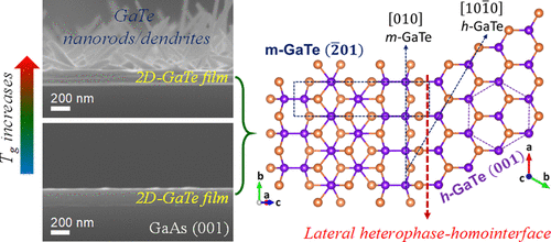
Molecular beam epitaxy of two-dimensional (2D) GaTe nanostructures on GaAs(001) substrates has been reported in this study. A trade-off between growth temperature and growth time (thickness) is a prerequisite for governing the crystal morphology of 2D GaTe materials from 2D epitaxial thin films to pseudo-one-dimensional (1D)/2D nanostructures (including nanorods, nanotriangles, and nanodendrites). Importantly, through real-time azimuthal reflection high-energy electron diffraction, a coexistence of hexagonal-GaTe (h-GaTe) and monoclinic-GaTe (m-GaTe) phases in the film was explored, corresponding to formation of lateral h/m-GaTe heterophase homojunctions. In addition, we found that utilizing a GaN/sapphire platform instead of the GaAs(001) substrate promotes formation of a single-phase h-GaTe in the thin film, which could be due to the surface-symmetry matching between the GaN/sapphire platform and the h-GaTe phase. Together with observing an asymmetric emission broad band of ∼1.76 eV that comes from the pseudo-1D m-GaTe phase, we provide convincing evidence that the emission feature located at 1.46 eV originates from the near-band-edge emission of the 2D h-GaTe epitaxial thin film. These results are meaningful in providing practical schemes to control the crystal phases of 2D GaTe materials and realize either hexagonal–monoclinic heterophase lateral homojunctions or single-phase h-GaTe epitaxial thin films on a wafer scale for future functional (opto)electronic devices, especially for near-infrared photodetectors.
中文翻译:

GaAs(001) 衬底上二维 GaTe 纳米结构的分子束外延:对近红外光电检测的影响
本研究报道了 GaAs(001) 衬底上二维 (2D) GaTe 纳米结构的分子束外延。生长温度和生长时间(厚度)之间的权衡是控制从 2D 外延薄膜到伪一维 (1D)/2D 纳米结构(包括纳米棒、纳米三角形和纳米枝晶)的 2D GaTe 材料晶体形态的先决条件)。重要的是,通过实时方位反射高能电子衍射,探索了六方-GaTe (h-GaTe) 和单斜-GaTe (m-GaTe) 相在薄膜中的共存,对应于横向 h/m- GaTe异相同质结。此外,我们发现利用 GaN/蓝宝石平台代替 GaAs(001) 衬底促进了薄膜中单相 h-GaTe 的形成,这可能是由于 GaN/蓝宝石平台和 h-GaTe 相之间的表面对称匹配。连同观察到来自伪 1D m-GaTe 相的~1.76 eV 的不对称发射宽带,我们提供了令人信服的证据,表明位于 1.46 eV 的发射特征源自 2D h-的近带边缘发射。氮化镓外延薄膜。这些结果对于提供实用的方案来控制 2D GaTe 材料的晶相和实现六方单斜异相横向同质结或单相 h-GaTe 外延薄膜在晶片规模上用于未来的功能(光)电子器件具有重要意义,尤其是用于近红外光电探测器。76 eV 来自伪 1D m-GaTe 相,我们提供了令人信服的证据,表明位于 1.46 eV 的发射特征源自 2D h-GaTe 外延薄膜的近带边缘发射。这些结果对于提供实用的方案来控制 2D GaTe 材料的晶相和实现六方单斜异相横向同质结或单相 h-GaTe 外延薄膜在晶片规模上用于未来的功能(光)电子器件具有重要意义,尤其是用于近红外光电探测器。76 eV 来自伪 1D m-GaTe 相,我们提供了令人信服的证据,表明位于 1.46 eV 的发射特征源自 2D h-GaTe 外延薄膜的近带边缘发射。这些结果对于提供实用的方案来控制 2D GaTe 材料的晶相和实现六方单斜异相横向同质结或单相 h-GaTe 外延薄膜在晶片规模上用于未来的功能(光)电子器件具有重要意义,尤其是用于近红外光电探测器。
更新日期:2021-09-24
中文翻译:
GaAs(001) 衬底上二维 GaTe 纳米结构的分子束外延:对近红外光电检测的影响
本研究报道了 GaAs(001) 衬底上二维 (2D) GaTe 纳米结构的分子束外延。生长温度和生长时间(厚度)之间的权衡是控制从 2D 外延薄膜到伪一维 (1D)/2D 纳米结构(包括纳米棒、纳米三角形和纳米枝晶)的 2D GaTe 材料晶体形态的先决条件)。重要的是,通过实时方位反射高能电子衍射,探索了六方-GaTe (h-GaTe) 和单斜-GaTe (m-GaTe) 相在薄膜中的共存,对应于横向 h/m- GaTe异相同质结。此外,我们发现利用 GaN/蓝宝石平台代替 GaAs(001) 衬底促进了薄膜中单相 h-GaTe 的形成,这可能是由于 GaN/蓝宝石平台和 h-GaTe 相之间的表面对称匹配。连同观察到来自伪 1D m-GaTe 相的~1.76 eV 的不对称发射宽带,我们提供了令人信服的证据,表明位于 1.46 eV 的发射特征源自 2D h-的近带边缘发射。氮化镓外延薄膜。这些结果对于提供实用的方案来控制 2D GaTe 材料的晶相和实现六方单斜异相横向同质结或单相 h-GaTe 外延薄膜在晶片规模上用于未来的功能(光)电子器件具有重要意义,尤其是用于近红外光电探测器。76 eV 来自伪 1D m-GaTe 相,我们提供了令人信服的证据,表明位于 1.46 eV 的发射特征源自 2D h-GaTe 外延薄膜的近带边缘发射。这些结果对于提供实用的方案来控制 2D GaTe 材料的晶相和实现六方单斜异相横向同质结或单相 h-GaTe 外延薄膜在晶片规模上用于未来的功能(光)电子器件具有重要意义,尤其是用于近红外光电探测器。76 eV 来自伪 1D m-GaTe 相,我们提供了令人信服的证据,表明位于 1.46 eV 的发射特征源自 2D h-GaTe 外延薄膜的近带边缘发射。这些结果对于提供实用的方案来控制 2D GaTe 材料的晶相和实现六方单斜异相横向同质结或单相 h-GaTe 外延薄膜在晶片规模上用于未来的功能(光)电子器件具有重要意义,尤其是用于近红外光电探测器。


 京公网安备 11010802027423号