Solar Energy Materials and Solar Cells ( IF 6.9 ) Pub Date : 2021-08-14 , DOI: 10.1016/j.solmat.2021.111325 O. Oklobia , G. Kartopu , S. Jones , P. Siderfin , B. Grew , H.K.H. Lee , W.C. Tsoi , Ali Abbas , J.M. Walls , D.L. McGott , M.O. Reese , S.J.C. Irvine
|
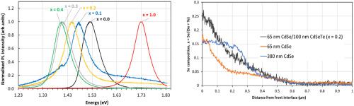
Recent developments in CdTe solar cell technology have included the incorporation of ternary alloy Cd(Se,Te) in the devices. CdTe absorber band gap grading due to Se alloying contributes to current density enhancement and can result in device performance improvement. Here we report Cd(Se,Te) polycrystalline thin films grown by a chamberless inline atmospheric pressure metal organic chemical vapour deposition technique, with subsequent incorporation in CdTe solar cells. The compositional dependence of the crystal structure and optical properties of Cd(Se,Te) are examined. Selenium graded Cd(Se,Te)/CdTe absorber structure in devices are demonstrated using either a single CdSe layer or CdSe/Cd(Se,Te) bilayer (with or without As doping in the Cd(Se,Te) layer). Cross-sectional TEM/EDS, photoluminescence spectra and secondary ion mass spectroscopy analysis confirmed the formation of a graded Se profile toward the back contact with a diffusion length of ~1.5 μm and revealed back-diffusion of Group V (As) dopants from the CdTe layer into Cd(Se,Te) grains. Due to the strong Se/Te interdiffusion, CdSe in the Se bilayer configuration was unable to form an n-type emitter layer in processed devices. In situ As doping of the Cd(Se,Te) layer benefited the device junction quality with current density reaching 28.3 mA/cm2. The results provide useful insights for the optimisation of Cd(Se,Te)/CdTe solar cells.
中文翻译:
MOCVD法开发用于薄膜太阳能电池的砷掺杂Cd(Se,Te)吸收剂
CdTe 太阳能电池技术的最新发展包括在器件中加入三元合金 Cd(Se,Te)。由于 Se 合金化导致的 CdTe 吸收体带隙分级有助于提高电流密度,并可以提高器件性能。在这里,我们报告了通过无室串联大气压金属有机化学气相沉积技术生长的 Cd(Se,Te) 多晶薄膜,随后并入 CdTe 太阳能电池。研究了 Cd(Se,Te) 的晶体结构和光学性质的组成依赖性。使用单个 CdSe 层或 CdSe/Cd(Se,Te) 双层(在 Cd(Se,Te) 层中掺杂或不掺杂 As)演示了器件中的硒渐变 Cd(Se,Te)/CdTe 吸收体结构。横截面 TEM/EDS,光致发光光谱和二次离子质谱分析证实了朝向背面接触的渐变 Se 分布的形成,扩散长度约为 1.5 μm,并揭示了 V 族 (As) 掺杂剂从 CdTe 层反向扩散到 Cd(Se,Te ) 谷物。由于强烈的 Se/Te 相互扩散,Se 双层结构中的 CdSe 无法在加工器件中形成 n 型发射极层。Cd(Se,Te) 层的原位 As 掺杂有利于器件结质量,电流密度达到 28.3 mA/cm Se 双层配置中的 CdSe 无法在加工器件中形成 n 型发射极层。Cd(Se,Te) 层的原位 As 掺杂有利于器件结质量,电流密度达到 28.3 mA/cm Se 双层配置中的 CdSe 无法在加工器件中形成 n 型发射极层。Cd(Se,Te) 层的原位 As 掺杂有利于器件结质量,电流密度达到 28.3 mA/cm2 . 结果为 Cd(Se,Te)/CdTe 太阳能电池的优化提供了有用的见解。


 京公网安备 11010802027423号