Microelectronic Engineering ( IF 2.3 ) Pub Date : 2021-08-13 , DOI: 10.1016/j.mee.2021.111613 Hongmin Youn 1 , Sunjung Kim 1 , Soo-Hyun Kim 2
|
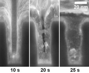
Direct copper (Cu) electrodeposition on a 10-nm atomic-layer-deposited (ALD) tungsten carbide (WC) diffusion barrier layer was investigated for building Cu interconnect in silicon (Si)-based microelectronic devices. The diffusion of Cu reducing species under potentiostatic Cu deposition was characterized according to applied cathodic potential in a neutral electrolyte with a concentration ratio of 1:10 for Cu to iminodiacetic acid (IDA) as a complexing agent. The diffusion-controlled nucleation and growth of Cu thin film on the ALD WC was figured out in relation to diffusion coefficients of Cu reducing species that were calculated from both modified current transient curves and more appropriately electrochemical impedance spectroscopy (EIS) analysis. At the end, the diffusion-controlled Cu fill of trenches with an aspect ratio of 6.3 and 15-nm bottom width was conducted by applying −1.4 V vs Ag/AgCl to an ALD-WC-covered, patterned Si wafer specimen.
中文翻译:
直接在用于铜互连的原子层沉积 WC 扩散阻挡层上电沉积 Cu 薄膜的扩散控制生长
研究了在 10 纳米原子层沉积 (ALD) 碳化钨 (WC) 扩散阻挡层上直接电沉积铜 (Cu) 以在硅 (Si) 基微电子器件中构建铜互连。在恒电位铜沉积下铜还原物质的扩散根据在中性电解质中施加的阴极电位表征,其中铜与亚氨基二乙酸(IDA)作为络合剂的浓度比为 1:10。ALD WC 上的 Cu 薄膜的扩散控制成核和生长与 Cu 还原物质的扩散系数有关,这些系数通过修改后的电流瞬态曲线和更合适的电化学阻抗谱 (EIS) 分析计算得出。最后,扩散控制的 Cu 填充深宽比为 6 的沟槽。对比Ag/AgCl 到 ALD-WC 覆盖的图案化硅晶片样品。


 京公网安备 11010802027423号