Materials Science in Semiconductor Processing ( IF 4.1 ) Pub Date : 2021-08-09 , DOI: 10.1016/j.mssp.2021.106126 J.L. Fuentes-Ríos 1 , D. Cabrera-German 1 , G. Suárez-Campos 1 , M.I. Pintor-Monroy 2 , H. Hu 3 , M.A. Quevedo-Lopez 1, 2 , M. Sotelo-Lerma 1
|
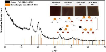
This work presents the development of a formulation for the synthesis of Pb1-xSnxS thin films by chemical bath deposition. The success of this formulation is due to the high miscibility between lead sulfide (PbS) and tin (II) sulfide (SnS). By adding different concentrations of a Pb2+ ions solution to a Sn2+ S2− formulation, we obtain Pb1-xSnxS films with different Pb/Sn ratio. The presence of Pb2+ in those films is confirmed by X-ray energy dispersive spectroscopy (EDS) and X-ray photoelectron spectroscopy (XPS). Structural analysis by X-ray diffraction (XDR) shows a crystalline phase change from an SnS orthorhombic structure (00.00 mmol Pb2+) to a solid solution where the orthorhombic and cubic structures coexist (30.00 mmol Pb2+), and finally reaching the formation of a cubic PbS structure. Changes in the morphology of the films are observed together with the incorporation of Pb2+ ions in the films, reducing the size of nano-flakes and becoming a more compact layer, leading to a decrease in the film thickness from 370 nm (00.00 mmol Pb2+) to 96 nm (50.00 mmol Pb2+). The decrease of the energy band gap (Eg) of the samples from 1.92 to 1.38 eV with the increase of the Pb2+ concentration is also observed, obtaining wide absorption spectra from visible to near-infrared.
中文翻译:
通过化学溶液沉积合成的 Pb1-xSnxS 薄膜中 Pb/Sn 比的调制
这项工作提出了通过化学浴沉积合成 Pb 1-x Sn x S 薄膜的配方的开发。该配方的成功归功于硫化铅 (PbS) 和硫化锡 (II) (SnS) 之间的高度混溶性。通过将不同浓度的 Pb 2+离子溶液添加到 Sn 2+ S 2−配方中,我们获得了具有不同 Pb/Sn 比的Pb 1-x Sn x S 薄膜。Pb 2+的存在X 射线能量色散谱 (EDS) 和 X 射线光电子能谱 (XPS) 证实了这些薄膜的存在。X 射线衍射 (XDR) 的结构分析显示,从 SnS 正交结构 (00.00 mmol Pb 2+ ) 到正交和立方结构共存的固溶体 (30.00 mmol Pb 2+ )的结晶相变,最终达到形成立方 PbS 结构。观察到薄膜形态的变化以及 Pb 2+离子在薄膜中的掺入,减小了纳米薄片的尺寸并成为更致密的层,导致薄膜厚度从 370 nm (00.00 mmol Pb 2+ ) 至 96 nm (50.00 mmol Pb 2+)。还观察到随着Pb 2+浓度的增加,样品的能带隙(Eg)从1.92eV减小到1.38eV ,获得了从可见光到近红外的宽吸收光谱。


 京公网安备 11010802027423号