当前位置:
X-MOL 学术
›
Phys. Rev. Appl.
›
论文详情
Our official English website, www.x-mol.net, welcomes your feedback! (Note: you will need to create a separate account there.)
Thermal Conductivity of Diamond Mosaic Crystals Grown by Chemical Vapor Deposition: Thermal Resistance of Junctions
Physical Review Applied ( IF 4.6 ) Pub Date : 2021-07-20 , DOI: 10.1103/physrevapplied.16.014049 V.G. Ralchenko 1, 2, 3 , A.V. Inyushkin 4 , Guoyang Shu 1, 2 , Bing Dai 1 , I.A. Karateev 4 , A.P. Bolshakov 1, 2, 3 , A.A. Khomich 2, 5 , E.E. Ashkinazi 2 , E.V. Zavedeev 2 , Jiecai Han 1 , Jiaqi Zhu 1
Physical Review Applied ( IF 4.6 ) Pub Date : 2021-07-20 , DOI: 10.1103/physrevapplied.16.014049 V.G. Ralchenko 1, 2, 3 , A.V. Inyushkin 4 , Guoyang Shu 1, 2 , Bing Dai 1 , I.A. Karateev 4 , A.P. Bolshakov 1, 2, 3 , A.A. Khomich 2, 5 , E.E. Ashkinazi 2 , E.V. Zavedeev 2 , Jiecai Han 1 , Jiaqi Zhu 1
Affiliation
|
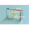
Large-area single-crystal “mosaic” diamond wafers, produced by homoepitaxial diamond chemical vapor deposition (CVD) on seed crystals aligned in close proximity, are of increasing interest for high-power electronic and optical applications, not least due to their extraordinary thermal properties. However, thermal conductivity might be reduced if a significant thermal-barrier resistance (TBR) forms on junctions between the single-crystal blocks of the mosaic. Here, using a steady-state longitudinal heat-flow method, we measure with a high accuracy the in-plane thermal conductivity in the broad temperature range of 6–410 K for a diamond mosaic crystal grown by microwave plasma CVD. At room temperature, the conductivity as high as is determined within a single block, reducing by less than 2% only for measured across the junction due to low enough TBR of approximately . However, below 100 K the TBR strongly increases with the temperature decrease, resulting in a dramatic reduction of the mosaic thermal conductivity compared to that for the single-crystal block. We associate the appearance of TBR with a layer (approximately equal to thick) of defected and stress material near the junction, as revealed with a confocal Raman mapping and transmission electron microscopy. The phonon scattering from defects in the zone around the junction strongly reduces the local thermal conductivity, as confirmed by modeling of heat transport. The observed temperature dependence of the local conductivity at K suggests the dominance of the phonon-dislocation scattering among other scattering processes. Our results show that the diamond mosaics preserve excellent thermal properties of the constituent single-crystal blocks at room and higher temperatures, and can be effectively used in the applications where the thermal conductivity is of primary relevance.
中文翻译:

通过化学气相沉积生长的金刚石镶嵌晶体的热导率:结的热阻
大面积单晶“镶嵌”金刚石晶片,由同质外延金刚石化学气相沉积 (CVD) 在紧密排列的籽晶上生产,在高功率电子和光学应用中越来越受到关注,尤其是因为它们具有非凡的耐热性。特性。然而,如果在马赛克的单晶块之间的结上形成显着的热障电阻 (TBR),则热导率可能会降低。在这里,我们使用稳态纵向热流方法,高精度地测量面内热导率在 6-410 K 的宽温度范围内,通过微波等离子体 CVD 生长的金刚石镶嵌晶体。在室温下,电导率高达 在单个块内确定,仅减少不到 2% 由于足够低的 TBR 大约在结点上测量 . 然而,在 100 K 以下,TBR 随着温度的降低而强烈增加,导致与单晶块相比,镶嵌导热系数显着降低。我们将 TBR 的外观与一个层(大约等于厚)的结点附近的缺陷和应力材料,如共焦拉曼映射和透射电子显微镜所示。正如热传输建模所证实的那样,来自结周围区域中的缺陷的声子散射强烈降低了局部热导率。观察到的温度依赖性 的局部电导率在 K 表明声子位错散射在其他散射过程中占主导地位。我们的结果表明,金刚石镶嵌物在室温和更高的温度下保持了组成单晶块的优异热性能,并且可以有效地用于热导率主要相关的应用中。
更新日期:2021-07-20
中文翻译:
通过化学气相沉积生长的金刚石镶嵌晶体的热导率:结的热阻
大面积单晶“镶嵌”金刚石晶片,由同质外延金刚石化学气相沉积 (CVD) 在紧密排列的籽晶上生产,在高功率电子和光学应用中越来越受到关注,尤其是因为它们具有非凡的耐热性。特性。然而,如果在马赛克的单晶块之间的结上形成显着的热障电阻 (TBR),则热导率可能会降低。在这里,我们使用稳态纵向热流方法,高精度地测量面内热导率在 6-410 K 的宽温度范围内,通过微波等离子体 CVD 生长的金刚石镶嵌晶体。在室温下,电导率高达 在单个块内确定,仅减少不到 2% 由于足够低的 TBR 大约在结点上测量 . 然而,在 100 K 以下,TBR 随着温度的降低而强烈增加,导致与单晶块相比,镶嵌导热系数显着降低。我们将 TBR 的外观与一个层(大约等于厚)的结点附近的缺陷和应力材料,如共焦拉曼映射和透射电子显微镜所示。正如热传输建模所证实的那样,来自结周围区域中的缺陷的声子散射强烈降低了局部热导率。观察到的温度依赖性 的局部电导率在 K 表明声子位错散射在其他散射过程中占主导地位。我们的结果表明,金刚石镶嵌物在室温和更高的温度下保持了组成单晶块的优异热性能,并且可以有效地用于热导率主要相关的应用中。


 京公网安备 11010802027423号