Engineering Science and Technology, an International Journal ( IF 5.7 ) Pub Date : 2021-07-10 , DOI: 10.1016/j.jestch.2021.06.015 Abhishek Kumar 1 , Santosh Kumar Gupta 1 , Vijaya Bhadauria 1
|
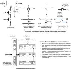
A 12-bit partial segmented current steering digital to analog converter (DAC) with low glitch area, power consumption, and integral nonlinearity (INL) error is proposed in this work. The cause of the glitch area and its possible solutions are explored. A current-mode logic (CML) latch with reduced output swing (Vdd to slightly below threshold voltage) is used at the input to the differential switch which reduces the glitch area (also known as glitch energy) significantly to 0.25 pVs. Further, this latch is used in the digital block of the proposed DAC to reduce the area and power requirement of the overall design. A dummy switch is used at the output of the differential switch to diminish effect of charge feedthrough at the output node of a current steering DAC. It also helps in the reduction of minimum allowable voltage headroom as compared to conventional double cascode structure and reduction of total power consumption to 9.1 mW operating at 200 MHz. The design and simulation of current steering DAC are performed in a 0.18 μm standard CMOS technology library using Cadence Virtuoso tool with a supply voltage of 1.8 V.
中文翻译:
低功耗和低毛刺面积电流转向 DAC
在这项工作中提出了一种具有低毛刺面积、功耗和积分非线性 (INL) 误差的 12 位部分分段电流控制数模转换器 (DAC)。探讨了故障区域的原因及其可能的解决方案。具有减小的输出摆幅 (V dd到略低于阈值电压)用于差分开关的输入,这将毛刺面积(也称为毛刺能量)显着降低到 0.25 pV。此外,该锁存器用于建议的 DAC 的数字模块,以减少整体设计的面积和功率要求。在差分开关的输出端使用了一个虚拟开关,以减少电流控制 DAC 输出节点处电荷馈通的影响。与传统的双共源共栅结构相比,它还有助于降低最小允许电压余量,并将总功耗降低到 200 MHz 下的 9.1 mW。在0.18进行电流导引DAC的设计和模拟 μ中号使用Cadence的Virtuoso工具与1.8伏的电源电压标准CMOS技术库


 京公网安备 11010802027423号