Our official English website, www.x-mol.net, welcomes your feedback! (Note: you will need to create a separate account there.)
Reconfigurable Parametric Amplifications of Spoof Surface Plasmons
Advanced Science ( IF 15.1 ) Pub Date : 2021-07-04 , DOI: 10.1002/advs.202100795 Xinxin Gao 1, 2, 3 , Jingjing Zhang 1, 2, 3 , Yu Luo 4 , Qian Ma 1, 2, 3 , Guo Dong Bai 1, 2 , Hao Chi Zhang 1, 2, 3 , Tie Jun Cui 1, 2, 3
Advanced Science ( IF 15.1 ) Pub Date : 2021-07-04 , DOI: 10.1002/advs.202100795 Xinxin Gao 1, 2, 3 , Jingjing Zhang 1, 2, 3 , Yu Luo 4 , Qian Ma 1, 2, 3 , Guo Dong Bai 1, 2 , Hao Chi Zhang 1, 2, 3 , Tie Jun Cui 1, 2, 3
Affiliation
|
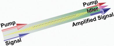
Next-generation inter-chip communication requires ultrafast ultra-compact interconnects. Designer plasmonics offers a possible route towards this goal. Further development of the plasmonic technique to circuit applications requires the direct amplification of plasmonic signals on a compact platform. However, significant signal distortions and limited operational speeds prevent the application of traditional MOS-based amplifiers to plasmonics. Up to day, the amplification of surface plasmons without phase distortion has remained a scientific challenge. In this work, the concept of parametric amplification (PA) is transplanted to the plasmonics and is realized experimentally an ultrathin reconfigurable PA using a spoof surface plasmon polariton (SSPP) waveguide integrated with tunable and nonlinear varactors. The measured parametric gain in the experiment can reach up to 9.14 dB within a short nonlinear propagation length, for example, six SSPP wavelengths, in excellent agreement with the theoretical prediction. By tuning the bias voltage of varactors, the phase-matching condition can be precisely controlled over a broad frequency band, enabling the authors to realize the multi-frequency PA of plasmonic signals. Measured phase responses confirm that the plasmonic parametric amplifier can significantly suppress the signal distortions as compared with the traditional MOS-based amplifier, which is a property highly desired for ultrafast wireless communication systems and integrated circuits.
中文翻译:

欺骗表面等离子体的可重构参数放大
下一代芯片间通信需要超快的超紧凑互连。设计师等离子体提供了实现这一目标的可能途径。等离子体技术在电路应用中的进一步发展需要在紧凑的平台上直接放大等离子体信号。然而,显着的信号失真和有限的运行速度阻碍了传统的基于 MOS 的放大器在等离子体中的应用。直到今天,没有相位失真的表面等离子体放大仍然是一个科学挑战。在这项工作中,参数放大 (PA) 的概念被移植到等离子体激元中,并使用与可调和非线性变容二极管集成的欺骗表面等离子体激元 (SSPP) 波导通过实验实现了超薄可重构 PA。实验中测得的参数增益在较短的非线性传播长度(例如 6 个 SSPP 波长)内可达到 9.14 dB,与理论预测非常吻合。通过调节变容二极管的偏置电压,可以在很宽的频带内精确控制相位匹配条件,使作者能够实现等离子体信号的多频 PA。测量的相位响应证实,与传统的基于 MOS 的放大器相比,等离子体参量放大器可以显着抑制信号失真,这是超快无线通信系统和集成电路非常需要的特性。通过调节变容二极管的偏置电压,可以在很宽的频带内精确控制相位匹配条件,使作者能够实现等离子体信号的多频 PA。测量的相位响应证实,与传统的基于 MOS 的放大器相比,等离子体参量放大器可以显着抑制信号失真,这是超快无线通信系统和集成电路非常需要的特性。通过调节变容二极管的偏置电压,可以在很宽的频带内精确控制相位匹配条件,使作者能够实现等离子体信号的多频 PA。测量的相位响应证实,与传统的基于 MOS 的放大器相比,等离子体参量放大器可以显着抑制信号失真,这是超快无线通信系统和集成电路非常需要的特性。
更新日期:2021-09-09
中文翻译:
欺骗表面等离子体的可重构参数放大
下一代芯片间通信需要超快的超紧凑互连。设计师等离子体提供了实现这一目标的可能途径。等离子体技术在电路应用中的进一步发展需要在紧凑的平台上直接放大等离子体信号。然而,显着的信号失真和有限的运行速度阻碍了传统的基于 MOS 的放大器在等离子体中的应用。直到今天,没有相位失真的表面等离子体放大仍然是一个科学挑战。在这项工作中,参数放大 (PA) 的概念被移植到等离子体激元中,并使用与可调和非线性变容二极管集成的欺骗表面等离子体激元 (SSPP) 波导通过实验实现了超薄可重构 PA。实验中测得的参数增益在较短的非线性传播长度(例如 6 个 SSPP 波长)内可达到 9.14 dB,与理论预测非常吻合。通过调节变容二极管的偏置电压,可以在很宽的频带内精确控制相位匹配条件,使作者能够实现等离子体信号的多频 PA。测量的相位响应证实,与传统的基于 MOS 的放大器相比,等离子体参量放大器可以显着抑制信号失真,这是超快无线通信系统和集成电路非常需要的特性。通过调节变容二极管的偏置电压,可以在很宽的频带内精确控制相位匹配条件,使作者能够实现等离子体信号的多频 PA。测量的相位响应证实,与传统的基于 MOS 的放大器相比,等离子体参量放大器可以显着抑制信号失真,这是超快无线通信系统和集成电路非常需要的特性。通过调节变容二极管的偏置电压,可以在很宽的频带内精确控制相位匹配条件,使作者能够实现等离子体信号的多频 PA。测量的相位响应证实,与传统的基于 MOS 的放大器相比,等离子体参量放大器可以显着抑制信号失真,这是超快无线通信系统和集成电路非常需要的特性。


 京公网安备 11010802027423号