Microelectronic Engineering ( IF 2.3 ) Pub Date : 2021-06-25 , DOI: 10.1016/j.mee.2021.111591 Taeyong Kim , Donggi Shin , Jinsu Park , Duy Phong Pham , Junsin Yi
|
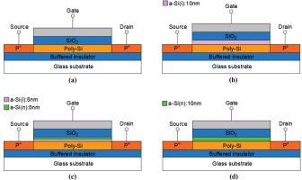
Low-temperature polycrystalline Si (LTPS) has been widely used to achieve large-area and high-speed TFT devices. In this regard, the enhancement in the mobility and stability of LTPS TFTs was investigated with the insertion of amorphous silicon (a-Si:H) capping layers at the insulator/poly-Si junction. Prior to capping layer deposition, the polycrystalline Si active region was plasma pre-treated under N2O or NH3/N2O ambience to refine the device characteristics. A high field effect mobility (μFE) of 90 cm2/Vs with a subthreshold swing (SS) of 1.21 V/dec was obtained from N2O treated non-capped LTPS TFT. The inclusion of a-Si:H(n)/a-Si:H(i) stacked capping layer at the gate insulator/poly-Si junction enhanced μFE to 152 cm2/Vs and decreased the SS to 0.69 V/dec. In contrast, the single capping layer of a-Si:H(i) and a-Si:H(n) showed feeble μFE improvements. The mechanism behind the μFE increase for the a-Si:H(n)/a-Si:H(i) stacked capping layer was explained using the atlas TCAD simulator. The grain boundary trap (Ntrap) density also decreased drastically with the insertion of the capping layer. A low and stable Ntrap value of 3.8 × 1011 cm−3 was obtained for a-Si:H(n)/a-Si:H(i) stacked capping layer with N2O pre-treatment, which may play a major role in enhancing the mobility and can be implemented for next-generation LTPS TFTs.
中文翻译:
使用堆叠覆盖层提高 LTPS 薄膜晶体管的迁移率
低温多晶硅(LTPS)已被广泛用于实现大面积和高速TFT器件。在这方面,通过在绝缘体/多晶硅结处插入非晶硅 (a-Si:H) 覆盖层,研究了 LTPS TFT 迁移率和稳定性的增强。在覆盖层沉积之前,多晶硅有源区在 N 2 O 或 NH 3 /N 2 O 环境下进行等离子体预处理以改进器件特性。从 N 2获得了 90 cm 2 /Vs的高场效应迁移率 (μ FE ) 和 1.21 V/dec 的亚阈值摆幅 (SS)O 处理的未封端的 LTPS TFT。在栅极绝缘体/多晶硅结处包含 a-Si:H(n)/a-Si:H(i) 堆叠覆盖层将 μ FE提高到 152 cm 2 /Vs 并将 SS 降低到 0.69 V/dec . 相比之下,a-Si:H(i) 和 a-Si:H(n) 的单个覆盖层显示出微弱的μFE改进。使用 atlas TCAD 模拟器解释了 a-Si:H(n)/a-Si:H(i) 堆叠覆盖层的μFE增加背后的机制。随着覆盖层的插入,晶界陷阱(N trap)密度也急剧下降。低且稳定的 N陷阱值 3.8 × 10 11 cm -3通过 N 2 O 预处理获得 a-Si:H(n)/a-Si:H(i) 堆叠盖层,这可能在提高迁移率方面起主要作用,并可用于下一代 LTPS薄膜晶体管。


 京公网安备 11010802027423号