当前位置:
X-MOL 学术
›
Phys. Status Solidi A
›
论文详情
Our official English website, www.x-mol.net, welcomes your feedback! (Note: you will need to create a separate account there.)
The Effect of Nanometer-Scale V-Pit Layer on the Carrier Recombination Mechanisms and Efficiency Droop of GaN-Based Green Light-Emitting Diodes
Physica Status Solidi (A) - Applications and Materials Science ( IF 2 ) Pub Date : 2021-06-25 , DOI: 10.1002/pssa.202100070 Chuanyu Jia 1 , Xiduo Hu 1 , Qi Wang 2 , Zhiwen Liang 2
Physica Status Solidi (A) - Applications and Materials Science ( IF 2 ) Pub Date : 2021-06-25 , DOI: 10.1002/pssa.202100070 Chuanyu Jia 1 , Xiduo Hu 1 , Qi Wang 2 , Zhiwen Liang 2
Affiliation
|
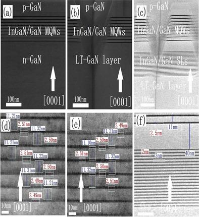
The effects of nanometer-scale V-pits layer with different parameters on the carrier recombination mechanisms and efficiency droop of GaN-based green light-emitting diodes (LEDs) are investigated. Under optimized growth conditions, the threading dislocations (TDs) are surrounded by V-pits layer with six (10–11) side wall facets. The V-pits layer contains sidewall multiple quantum wells (MQWs) with bandgap several hundred millielectronvolts higher than that of c-plane MQWs. This higher bandgap acts as a barrier for carriers and prevents them from reaching the dislocations, which can effectively suppress the nonradiative recombination. Analysis suggests that the V-pits enhance hole injection into deeper MQWs, which is confirmed by the secondary ion mass spectroscopy profiles of Mg and Al. With the aid of the V-pits layer, holes can be injected into deeper MQWs, which reduce the carrier concentration within individual QWs. Therefore, the Auger-related efficiency droop can be suppressed. The results show that LED with 200 nm LT-GaN + 40 nm n-GaN V-pits layer is able to deliver an improvement in the light output power by 189% as compared with reference LED without V-pits layer. At 200 mA, the efficiency droop for LED with200 nm LT-GaN + 40 nm n-GaN V-pits is 25.9%, which is much smaller than 34.7% for reference LED without V-pits.
中文翻译:

纳米级 V-Pit 层对 GaN 基绿色发光二极管载流子复合机制和效率下降的影响
研究了不同参数的纳米级 V 坑层对 GaN 基绿色发光二极管 (LED) 载流子复合机制和效率下降的影响。在优化的生长条件下,穿透位错 (TD) 被具有六个 (10-11) 侧壁面的 V 凹坑层包围。V 坑层包含侧壁多量子阱 (MQW),其带隙比c 的带隙高数百毫电子伏特-平面 MQW。这种较高的带隙作为载流子的屏障,阻止它们到达位错,可以有效地抑制非辐射复合。分析表明 V 凹坑增强了空穴注入更深的 MQW,这由 Mg 和 Al 的二次离子质谱图证实。借助 V 坑层,可以将空穴注入更深的 MQW,从而降低单个 QW 内的载流子浓度。因此,可以抑制与俄歇相关的效率下降。结果表明,与没有 V 坑层的参考 LED 相比,具有 200 nm LT-GaN + 40 nm n-GaN V 坑层的 LED 能够将光输出功率提高 189%。在 200 mA 时,具有 200 nm LT-GaN + 40 nm n-GaN V 凹坑的 LED 的效率下降为 25.9%,远小于 34。
更新日期:2021-06-25
中文翻译:
纳米级 V-Pit 层对 GaN 基绿色发光二极管载流子复合机制和效率下降的影响
研究了不同参数的纳米级 V 坑层对 GaN 基绿色发光二极管 (LED) 载流子复合机制和效率下降的影响。在优化的生长条件下,穿透位错 (TD) 被具有六个 (10-11) 侧壁面的 V 凹坑层包围。V 坑层包含侧壁多量子阱 (MQW),其带隙比c 的带隙高数百毫电子伏特-平面 MQW。这种较高的带隙作为载流子的屏障,阻止它们到达位错,可以有效地抑制非辐射复合。分析表明 V 凹坑增强了空穴注入更深的 MQW,这由 Mg 和 Al 的二次离子质谱图证实。借助 V 坑层,可以将空穴注入更深的 MQW,从而降低单个 QW 内的载流子浓度。因此,可以抑制与俄歇相关的效率下降。结果表明,与没有 V 坑层的参考 LED 相比,具有 200 nm LT-GaN + 40 nm n-GaN V 坑层的 LED 能够将光输出功率提高 189%。在 200 mA 时,具有 200 nm LT-GaN + 40 nm n-GaN V 凹坑的 LED 的效率下降为 25.9%,远小于 34。


 京公网安备 11010802027423号