当前位置:
X-MOL 学术
›
Int. J. Circ. Theory Appl.
›
论文详情
Our official English website, www.x-mol.net, welcomes your feedback! (Note: you will need to create a separate account there.)
An input controlled leakage restrainer transistor-based technique for leakage and short-circuit power reduction of 1-bit hybrid full adders
International Journal of Circuit Theory and Applications ( IF 2.3 ) Pub Date : 2021-06-08 , DOI: 10.1002/cta.3053 Mohammad Moradinezhad Maryan 1 , Majid Amini‐Valashani 1 , Seyed Javad Azhari 1
International Journal of Circuit Theory and Applications ( IF 2.3 ) Pub Date : 2021-06-08 , DOI: 10.1002/cta.3053 Mohammad Moradinezhad Maryan 1 , Majid Amini‐Valashani 1 , Seyed Javad Azhari 1
Affiliation
|
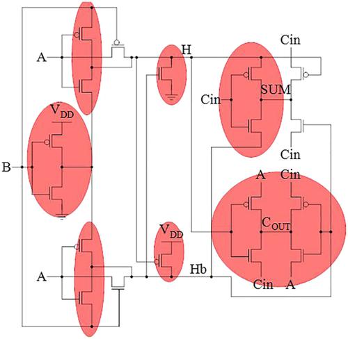
The sharp increase in the leakage part of the total power of the very large scale integration (VLSI) circuits is a significant concern in the deep submicron CMOS process. The NOT gates, Gate Diffusion Input (GDI) cells, restorer NMOS–PMOS transistors for full-swing operation, and any path from the power voltage to the ground are the main sources of leakage power dissipation as well as short-circuit in the VLSI CMOS circuits/chips. The input controlled leakage restrainer transistor (ICLRT) is a new circuit-level method that is proposed in this paper. The ICLRTs can be deliberately added to any VLSI CMOS circuit to largely diminish the total power dissipation especially by the reduction of its leakage and short-circuit parts. The full adders are vital parts in various VLSI circuits/systems, especially in circuits used for fulfilling arithmetic operations. Those are often placed in the critical paths for multiplication and division, so influence the throughout the efficiency of the system. To test the proposed technique, ICLRTs added to five best 1-bit hybrid full adders in the deep submicron process to fit the needs of the day. The efficiency of the proposed method is evaluated using SPICE simulations in 22-nm CMOS BSIM4 process. Evaluation outcomes with 1-V power supply verified that the power dissipation and power-delay product (PDP) of the hybrid full adders based on ICLRT technique relative to corresponding original designs are reduced 65.67–95.7% and 35.85–87.37%, respectively. Mismatch analysis and Monte Carlo simulations prove the robustness and stability of the presented circuits in the presence of the process, voltage, and temperature (PVT) variations.
中文翻译:

一种基于输入控制的泄漏抑制器晶体管技术,用于降低 1 位混合全加器的泄漏和短路功率
超大规模集成 (VLSI) 电路总功率中泄漏部分的急剧增加是深亚微米 CMOS 工艺中的一个重要问题。NOT 门、栅极扩散输入 (GDI) 单元、用于全摆幅操作的恢复器 NMOS-PMOS 晶体管以及从电源电压到地的任何路径都是 VLSI 中泄漏功耗和短路的主要来源CMOS 电路/芯片。输入控制泄漏抑制晶体管(ICLRT)是本文提出的一种新的电路级方法。ICLRT 可以有意添加到任何 VLSI CMOS 电路中,以大幅降低总功耗,尤其是通过减少其泄漏和短路部分。全加器是各种 VLSI 电路/系统中的重要部件,特别是在用于实现算术运算的电路中。这些通常被放置在乘法和除法的关键路径中,因此影响系统的整体效率。为了测试所提出的技术,ICLRT 在深亚微米工艺中添加到五个最好的 1 位混合全加器以满足当今的需求。在 22-nm CMOS BSIM4 工艺中使用 SPICE 模拟评估了所提出方法的效率。1-V 电源的评估结果证实,基于 ICLRT 技术的混合全加器的功耗和功率延迟积 (PDP) 相对于相应的原始设计分别降低了 65.67-95.7% 和 35.85-87.37%。失配分析和蒙特卡罗模拟证明了所提出电路在存在工艺、电压、
更新日期:2021-08-12
中文翻译:
一种基于输入控制的泄漏抑制器晶体管技术,用于降低 1 位混合全加器的泄漏和短路功率
超大规模集成 (VLSI) 电路总功率中泄漏部分的急剧增加是深亚微米 CMOS 工艺中的一个重要问题。NOT 门、栅极扩散输入 (GDI) 单元、用于全摆幅操作的恢复器 NMOS-PMOS 晶体管以及从电源电压到地的任何路径都是 VLSI 中泄漏功耗和短路的主要来源CMOS 电路/芯片。输入控制泄漏抑制晶体管(ICLRT)是本文提出的一种新的电路级方法。ICLRT 可以有意添加到任何 VLSI CMOS 电路中,以大幅降低总功耗,尤其是通过减少其泄漏和短路部分。全加器是各种 VLSI 电路/系统中的重要部件,特别是在用于实现算术运算的电路中。这些通常被放置在乘法和除法的关键路径中,因此影响系统的整体效率。为了测试所提出的技术,ICLRT 在深亚微米工艺中添加到五个最好的 1 位混合全加器以满足当今的需求。在 22-nm CMOS BSIM4 工艺中使用 SPICE 模拟评估了所提出方法的效率。1-V 电源的评估结果证实,基于 ICLRT 技术的混合全加器的功耗和功率延迟积 (PDP) 相对于相应的原始设计分别降低了 65.67-95.7% 和 35.85-87.37%。失配分析和蒙特卡罗模拟证明了所提出电路在存在工艺、电压、


 京公网安备 11010802027423号