Journal of Physics and Chemistry of Solids ( IF 4 ) Pub Date : 2021-06-04 , DOI: 10.1016/j.jpcs.2021.110197 Mohd Shkir , Mohd Taukeer Khan , H. Elhosiny Ali , El Sayed Yousef , H. Algarni , S. AlFaify
|
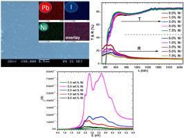
Herein, thin films of PbI2 with different Ni-doping concentrations (0.0, 1.0, 3.0, 5.0 and 7.5 wt%) have been fabricated using spin coating method. The fabricated films possess a hexagonal crystalline structure and growth along the (001) plane, as-confirmed by XRD analysis. EDS elemental-mapping confirmed the uniform doping of Ni throughout the PbI2 films. SEM images reveal the formation of nanoparticles/sheets with sizes of ⁓100 nm in the fabricated films. An optical absorption study reveal the change in absorption edge of PbI2 observed upon Ni doping. The fabricated films are highly transparent (i.e. 80–86%) in the visible to near-infra red region. The energy gap of PbI2 was determined to be 2.34 eV, which increased to 2.45 eV for the 5 wt% Ni@PbI2 film. The fabricated films show photoluminescence quenching when doped with Ni. The refractive index values were determine to be between 1.73 to 3.37 in the whole region studied. Furthermore, the dielectric-electrical-non-linear optical parameters were also determined. The , and values were estimated to be in range of 0.16–0.83, 1.1 × 10⁻¹³ to 7.8 × 10⁻¹¹ esu and 2.3 × 10⁻¹² to 8.7 × 10⁻¹⁰ esu, respectively. It was noticed that these parameters were enhanced upon Ni doping up to 5.0 wt%. The enhanced opto-non-linear properties of PbI2 by Ni doping makes it a suitable candidate for optoelectronic applications.
中文翻译:
用于高阶非线性应用的低成本沉积纯和 Ni@PbI2/玻璃纳米结构薄膜的增强光非线性特性
在此,使用旋涂法制备了具有不同 Ni 掺杂浓度(0.0、1.0、3.0、5.0 和 7.5 wt%)的 PbI 2薄膜。XRD 分析证实,制造的薄膜具有六边形晶体结构和沿 (001) 面生长。EDS 元素映射证实了整个 PbI 2薄膜中 Ni 的均匀掺杂。SEM 图像显示在制造的薄膜中形成了尺寸为⁓100 nm 的纳米颗粒/薄片。光学吸收研究揭示了在 Ni 掺杂时观察到的 PbI 2吸收边缘的变化。制造的薄膜在可见光到近红外区域是高度透明的(即 80-86%)。PbI 2的能隙被确定为 2.34 eV,对于 5 wt% Ni@PbI 2薄膜增加到 2.45 eV 。当掺杂有 Ni 时,制造的薄膜显示出光致发光猝灭。在整个研究区域中,折射率值被确定为介于 1.73 到 3.37 之间。此外,还确定了介电-电-非线性光学参数。这, 和 估计值分别在 0.16–0.83、1.1 × 10 -13至 7.8 × 10 -11 esu 和 2.3 × 10 -12至 8.7 × 10 -10 esu 的范围内。注意到这些参数在 Ni 掺杂至 5.0 wt% 时得到增强。通过 Ni 掺杂增强的 PbI 2光非线性特性使其成为光电应用的合适候选者。


 京公网安备 11010802027423号