当前位置:
X-MOL 学术
›
Int. J. Circ. Theory Appl.
›
论文详情
Our official English website, www.x-mol.net, welcomes your feedback! (Note: you will need to create a separate account there.)
A 0.3–5 GHz, low-power, area-efficient, high dynamic range variable gain low-noise amplifier based on tunable active floating inductor technique
International Journal of Circuit Theory and Applications ( IF 2.3 ) Pub Date : 2021-06-02 , DOI: 10.1002/cta.3056 Farzaneh Soleymani 1 , Parviz Amiri 1 , Mohammad Hossein Maghami 1
International Journal of Circuit Theory and Applications ( IF 2.3 ) Pub Date : 2021-06-02 , DOI: 10.1002/cta.3056 Farzaneh Soleymani 1 , Parviz Amiri 1 , Mohammad Hossein Maghami 1
Affiliation
|
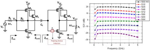
An area-efficient low-noise amplifier with extensive voltage gain variation in the frequency range of 0.3 to 5 GHz is proposed. The designed amplifier comprises of two stages of inverter cells, where by utilizing a resistance shunt feedback, the first stage makes the appropriate voltage gain and input impedance matching, and the second stage increases the bandwidth of the circuit utilizing an active floating inductor. Self-forward-body-bias structure is employed in the presented work for reducing power consumption and improving the overall circuit performance. High voltage gain, low power consumption, wide frequency range of operation, lack of physical inductor, and consequently small occupied active area are among the most important features of the proposed circuit. The presented amplifier has been designed and simulated in standard 90-nm and 0.18-μm technologies with 0.9- and 1.2-V supply voltages, respectively, in which important specifications are reported for 90-nm complementary metal–oxide semiconductor (CMOS) process in details. Power consumption of the designed amplifier is 8.8 mW in 90-nm technology with a flat variable voltage gain of −22 to 21.2 dB. The circuit consumes silicon area of 122 × 112 μm2, and in the high-gain mode, the simulated S11 parameter is less than −10 dB, noise figure is almost 3.2 dB, and the IIP3 is equal to −4 dBm.
中文翻译:

基于可调有源浮动电感技术的 0.3–5 GHz、低功耗、面积效率高、高动态范围可变增益低噪声放大器
提出了一种在 0.3 至 5 GHz 频率范围内具有广泛电压增益变化的面积效率低噪声放大器。设计的放大器由两级逆变器单元组成,其中第一级利用电阻分流反馈进行适当的电压增益和输入阻抗匹配,第二级利用有源浮动电感器增加电路的带宽。在所提出的工作中采用自前向体偏置结构来降低功耗并提高整体电路性能。高电压增益、低功耗、宽工作频率范围、没有物理电感器以及因此占用的有效面积小是所提出电路的最重要特征之一。所提出的放大器是在标准 90-nm 和 0 波长下设计和模拟的。分别具有 0.9V 和 1.2V 电源电压的 18-μm 技术,其中详细报告了 90-nm 互补金属氧化物半导体 (CMOS) 工艺的重要规格。采用 90-nm 技术设计的放大器的功耗为 8.8 mW,具有 -22 至 21.2 dB 的平坦可变电压增益。电路消耗硅面积为122×112μm如图2所示,在高增益模式下,模拟的S 11参数小于-10 dB,噪声系数接近3.2 dB,IIP3等于-4 dBm。
更新日期:2021-06-02
中文翻译:
基于可调有源浮动电感技术的 0.3–5 GHz、低功耗、面积效率高、高动态范围可变增益低噪声放大器
提出了一种在 0.3 至 5 GHz 频率范围内具有广泛电压增益变化的面积效率低噪声放大器。设计的放大器由两级逆变器单元组成,其中第一级利用电阻分流反馈进行适当的电压增益和输入阻抗匹配,第二级利用有源浮动电感器增加电路的带宽。在所提出的工作中采用自前向体偏置结构来降低功耗并提高整体电路性能。高电压增益、低功耗、宽工作频率范围、没有物理电感器以及因此占用的有效面积小是所提出电路的最重要特征之一。所提出的放大器是在标准 90-nm 和 0 波长下设计和模拟的。分别具有 0.9V 和 1.2V 电源电压的 18-μm 技术,其中详细报告了 90-nm 互补金属氧化物半导体 (CMOS) 工艺的重要规格。采用 90-nm 技术设计的放大器的功耗为 8.8 mW,具有 -22 至 21.2 dB 的平坦可变电压增益。电路消耗硅面积为122×112μm如图2所示,在高增益模式下,模拟的S 11参数小于-10 dB,噪声系数接近3.2 dB,IIP3等于-4 dBm。


 京公网安备 11010802027423号