当前位置:
X-MOL 学术
›
J. Appl. Crystallogr.
›
论文详情
Our official English website, www.x-mol.net, welcomes your feedback! (Note: you will need to create a separate account there.)
X-ray scattering profiles: revealing the porosity gradient in porous silicon
Journal of Applied Crystallography ( IF 6.1 ) Pub Date : 2021-05-25 , DOI: 10.1107/s1600576721003484 Cosmin Romanitan , Pericle Varasteanu , Daniela C. Culita , Alexandru Bujor , Oana Tutunaru
Journal of Applied Crystallography ( IF 6.1 ) Pub Date : 2021-05-25 , DOI: 10.1107/s1600576721003484 Cosmin Romanitan , Pericle Varasteanu , Daniela C. Culita , Alexandru Bujor , Oana Tutunaru
|
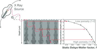
Porous silicon layers with different porosities were prepared by adjusting the anodization current density of the electrochemical etching process, starting from highly doped p-type crystalline silicon wafers. The microstructural parameters of the porous layers were assessed by high-resolution X-ray diffraction, total external reflection, scanning electron microscopy and nitrogen adsorption–desorption analysis. Furthermore, both the surface porosity and the mean porosity for the entire volume of the samples were estimated by employing total external reflection measurements and X-ray reciprocal-space mapping, respectively. The results clearly indicate that the surface porosity is different from the mean porosity, and the presence of a depth porosity gradient is suggested. To evaluate the porosity gradient in a nondestructive way, a new laboratory method using the grazing-incidence X-ray diffraction technique is reported. It is based on the analysis of the X-ray scattering profiles of the porous layers to obtain the static Debye–Waller factors. In this way, a description of the porosity gradient in a quantitative framework becomes possible, and, as a result, it was shown that the porosity increases exponentially with the X-ray penetration depth. Moreover, a strong dependence between the porosity gradient and the anodization current was demonstrated. Thus, in the case of the lowest anodization current (e.g. 50 mA cm−2) a variation of only 15% of the porosity from the surface to the interface is found, but when applying a high anodization current of 110 mA cm−2 the porosity close to the bulk interface is almost three times higher than at the surface.
中文翻译:

X 射线散射剖面:揭示多孔硅中的孔隙率梯度
通过调整电化学蚀刻工艺的阳极氧化电流密度,从高度掺杂的 p 型晶体硅晶片开始,制备具有不同孔隙率的多孔硅层。多孔层的微观结构参数通过高分辨率 X 射线衍射、全外反射、扫描电子显微镜和氮吸附-解吸分析进行评估。此外,通过分别采用全外反射测量和 X 射线倒易空间映射来估计整个样品体积的表面孔隙率和平均孔隙率。结果清楚地表明地表孔隙度不同于平均孔隙度,并且表明存在深度孔隙度梯度。为了以非破坏性的方式评估孔隙度梯度,报告了一种使用掠入射 X 射线衍射技术的新实验室方法。它基于对多孔层的 X 射线散射分布的分析,以获得静态德拜-沃勒因子。通过这种方式,在定量框架中描述孔隙度梯度成为可能,结果表明孔隙度随 X 射线穿透深度呈指数增长。此外,证明了孔隙率梯度和阳极氧化电流之间的强相关性。因此,在最低阳极氧化电流(在定量框架中描述孔隙度梯度成为可能,结果表明孔隙度随 X 射线穿透深度呈指数增加。此外,证明了孔隙率梯度和阳极氧化电流之间的强相关性。因此,在最低阳极氧化电流(在定量框架中描述孔隙度梯度成为可能,结果表明孔隙度随 X 射线穿透深度呈指数增加。此外,证明了孔隙率梯度和阳极氧化电流之间的强相关性。因此,在最低阳极氧化电流(例如50 mA cm -2 ) 发现从表面到界面的孔隙率变化仅为 15%,但是当施加 110 mA cm -2的高阳极氧化电流时,接近体界面的孔隙率几乎高出三倍比在表面上。
更新日期:2021-06-03
中文翻译:
X 射线散射剖面:揭示多孔硅中的孔隙率梯度
通过调整电化学蚀刻工艺的阳极氧化电流密度,从高度掺杂的 p 型晶体硅晶片开始,制备具有不同孔隙率的多孔硅层。多孔层的微观结构参数通过高分辨率 X 射线衍射、全外反射、扫描电子显微镜和氮吸附-解吸分析进行评估。此外,通过分别采用全外反射测量和 X 射线倒易空间映射来估计整个样品体积的表面孔隙率和平均孔隙率。结果清楚地表明地表孔隙度不同于平均孔隙度,并且表明存在深度孔隙度梯度。为了以非破坏性的方式评估孔隙度梯度,报告了一种使用掠入射 X 射线衍射技术的新实验室方法。它基于对多孔层的 X 射线散射分布的分析,以获得静态德拜-沃勒因子。通过这种方式,在定量框架中描述孔隙度梯度成为可能,结果表明孔隙度随 X 射线穿透深度呈指数增长。此外,证明了孔隙率梯度和阳极氧化电流之间的强相关性。因此,在最低阳极氧化电流(在定量框架中描述孔隙度梯度成为可能,结果表明孔隙度随 X 射线穿透深度呈指数增加。此外,证明了孔隙率梯度和阳极氧化电流之间的强相关性。因此,在最低阳极氧化电流(在定量框架中描述孔隙度梯度成为可能,结果表明孔隙度随 X 射线穿透深度呈指数增加。此外,证明了孔隙率梯度和阳极氧化电流之间的强相关性。因此,在最低阳极氧化电流(例如50 mA cm -2 ) 发现从表面到界面的孔隙率变化仅为 15%,但是当施加 110 mA cm -2的高阳极氧化电流时,接近体界面的孔隙率几乎高出三倍比在表面上。


 京公网安备 11010802027423号