Microelectronic Engineering ( IF 2.3 ) Pub Date : 2021-05-18 , DOI: 10.1016/j.mee.2021.111570 T.D. Vethaak , F. Gustavo , T. Farjot , T. Kubart , P. Gergaud , S.-L. Zhang , F. Lefloch , F. Nemouchi
|
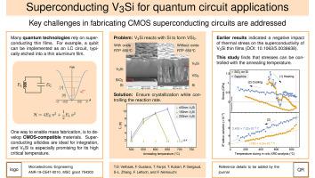
V3Si thin films are known to be superconducting with transition temperatures up to 15 K, depending on the annealing temperature and the properties of the substrate underneath. Here we investigate the film structural properties with the prospect of further integration in silicon technology for quantum circuits. Two challenges have been identified: (i) the large difference in thermal expansion coefficient between V3Si and the Si substrate leads to large thermal strains after thermal processing, and (ii) the undesired silicide phase VSi2 forms when V3Si is deposited on silicon. The first of these is studied by depositing layers of 200 nm V3Si on wafers of sapphire and oxidized silicon, neither of which react with the silicide. These samples are then heated and cooled between room temperature and 860 °C, during which in-situ XRD measurements are performed. Analysis reveals a highly non-linear stress development during heating with contributions from crystallization and subsequent grain growth, as well as the thermal expansion mismatch between silicide and substrate, while the film behaves thermoelastically during cooling. The second challenge is explored by depositing films of 20, 50, 100 and 200 nm of V3Si on bulk silicon. For each thickness, six samples are prepared, which are then annealed at temperatures between 500 and 750 °C, followed by measurements of their resistivity, residual resistance ratio and superconducting critical temperature. A process window is identified for silicide thicknesses of at least 100 nm, within which a trade-off needs to be made between the quality of the V3Si film and its consumption by the formation of VSi2.
中文翻译:
V 3 Si超导,用于量子电路应用
已知V 3 Si薄膜在高达15 K的转变温度下是超导的,具体取决于退火温度和下方衬底的性能。在这里,我们研究膜的结构特性,并有望进一步集成到量子电路的硅技术中。已经确定了两个挑战:(i)V 3 Si和Si衬底之间的热膨胀系数差异很大,导致热处理后的热应变很大;(ii)沉积V 3 Si时形成了不希望的硅化物相VSi 2在硅上。首先通过沉积200 nm V 3的层来研究蓝宝石和氧化硅晶片上的Si都不与硅化物反应。然后将这些样品在室温和860°C之间加热和冷却,在此期间执行原位XRD测量。分析表明,在加热过程中会产生高度非线性的应力,这归因于结晶和随后的晶粒长大,以及硅化物和基材之间的热膨胀失配,而薄膜在冷却过程中表现出热弹性。通过沉积V 3的20、50、100和200 nm的薄膜来探索第二个挑战Si在块状硅上。对于每种厚度,准备六个样品,然后在500至750°C的温度下进行退火,然后测量其电阻率,残余电阻比和超导临界温度。对于至少100nm的硅化物厚度,确定了工艺窗口,在该工艺窗口中,需要在V 3 Si膜的质量与其通过形成VSi 2的消耗之间进行权衡。


 京公网安备 11010802027423号