当前位置:
X-MOL 学术
›
Phys. Status Solidi. Rapid Res. Lett.
›
论文详情
Our official English website, www.x-mol.net, welcomes your feedback! (Note: you will need to create a separate account there.)
Optoelectronic Inactivity of Dislocations in Cu(In,Ga)Se2 Thin Films
Physica Status Solidi-Rapid Research Letters ( IF 2.8 ) Pub Date : 2021-05-13 , DOI: 10.1002/pssr.202100042 Daniel Abou-Ras 1 , Aleksandra Nikolaeva 1 , Maximilian Krause 1 , Lars Korte 1 , Helena Stange 1 , Roland Mainz 1 , Ekin Simsek Sanli 2 , Peter A. van Aken 2 , Takeyoshi Sugaya 3, 4 , Jiro Nishinaga 3, 4
Physica Status Solidi-Rapid Research Letters ( IF 2.8 ) Pub Date : 2021-05-13 , DOI: 10.1002/pssr.202100042 Daniel Abou-Ras 1 , Aleksandra Nikolaeva 1 , Maximilian Krause 1 , Lars Korte 1 , Helena Stange 1 , Roland Mainz 1 , Ekin Simsek Sanli 2 , Peter A. van Aken 2 , Takeyoshi Sugaya 3, 4 , Jiro Nishinaga 3, 4
Affiliation
|
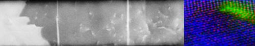
High-efficiency Cu(In,Ga)Se2 (CIGS) thin-film solar cells are based on polycrystalline CIGS absorber layers, which contain grain boundaries, stacking faults, and dislocations. While planar defects in CIGS layers have been investigated extensively, little is still known about the impact of dislocations on optoelectronic properties of CIGS absorbers. Herein, evidence for an optoelectronic inactivity of dislocations in these thin films is given, in contrast to the situation at grain boundaries. This unique behavior is explained by the extensive elemental redistribution detected around dislocation cores, which is connected with the dislocation strain field, probably leading to a shift of defect states toward the band edges.
中文翻译:

Cu(In,Ga)Se2薄膜中位错的光电惰性
高效 Cu(In,Ga)Se 2 (CIGS) 薄膜太阳能电池基于多晶 CIGS 吸收层,其中包含晶界、堆垛层错和位错。尽管已对 CIGS 层中的平面缺陷进行了广泛的研究,但关于位错对 CIGS 吸收体光电特性的影响仍知之甚少。在此,与晶界处的情况相比,给出了这些薄膜中位错的光电不活动的证据。这种独特的行为可以通过在位错核心周围检测到的广泛元素重新分布来解释,这与位错应变场有关,可能导致缺陷状态向带边缘移动。
更新日期:2021-07-12
中文翻译:
Cu(In,Ga)Se2薄膜中位错的光电惰性
高效 Cu(In,Ga)Se 2 (CIGS) 薄膜太阳能电池基于多晶 CIGS 吸收层,其中包含晶界、堆垛层错和位错。尽管已对 CIGS 层中的平面缺陷进行了广泛的研究,但关于位错对 CIGS 吸收体光电特性的影响仍知之甚少。在此,与晶界处的情况相比,给出了这些薄膜中位错的光电不活动的证据。这种独特的行为可以通过在位错核心周围检测到的广泛元素重新分布来解释,这与位错应变场有关,可能导致缺陷状态向带边缘移动。


 京公网安备 11010802027423号