当前位置:
X-MOL 学术
›
ACS Photonics
›
论文详情
Our official English website, www.x-mol.net, welcomes your feedback! (Note: you will need to create a separate account there.)
Enhanced Radiative Efficiency in GaN Nanowires Grown on Sputtered TiNx: Effects of Surface Electric Fields
ACS Photonics ( IF 7 ) Pub Date : 2021-05-12 , DOI: 10.1021/acsphotonics.1c00224 Thomas Auzelle 1 , Mani Azadmand 1 , Timur Flissikowski 1 , Manfred Ramsteiner 1 , Katrin Morgenroth 1 , Carsten Stemmler 1 , Sergio Fernández-Garrido 1 , Stefano Sanguinetti 2 , Holger T. Grahn 1 , Lutz Geelhaar 1 , Oliver Brandt 1
ACS Photonics ( IF 7 ) Pub Date : 2021-05-12 , DOI: 10.1021/acsphotonics.1c00224 Thomas Auzelle 1 , Mani Azadmand 1 , Timur Flissikowski 1 , Manfred Ramsteiner 1 , Katrin Morgenroth 1 , Carsten Stemmler 1 , Sergio Fernández-Garrido 1 , Stefano Sanguinetti 2 , Holger T. Grahn 1 , Lutz Geelhaar 1 , Oliver Brandt 1
Affiliation
|
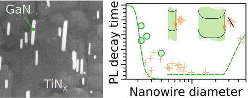
GaN nanowires grown by molecular beam epitaxy generally suffer from dominant nonradiative recombination, which is believed to originate from point defects. To suppress the formation of these defects, we explore the synthesis of GaN nanowires at temperatures up to 915 °C enabled by the use of thermally stable TiNx/Al2O3 substrates. These samples exhibit indeed bound exciton decay times approaching those measured for state-of-the-art bulk GaN. However, the decay time is not correlated with the growth temperature, but rather with the nanowire diameter. The inverse dependence of the decay time on diameter suggests that the nonradiative process in GaN nanowires is not controlled by the defect density, but by the field ionization of excitons in the radial electric field caused by surface band bending. We propose a unified mechanism accounting for nonradiative recombination in GaN nanowires of arbitrary diameter.
中文翻译:

在溅射的 TiN x上生长的 GaN 纳米线的增强辐射效率:表面电场的影响
通过分子束外延生长的 GaN 纳米线通常受到主要的非辐射复合的影响,这被认为是源于点缺陷。为了抑制这些缺陷的形成,我们探索了通过使用热稳定的 TiN x /Al 2 O 3在高达 915 °C 的温度下合成 GaN 纳米线基材。这些样品的束缚激子衰减时间确实接近于最先进的体 GaN 测量值。然而,衰减时间与生长温度无关,而是与纳米线直径相关。衰减时间与直径的反比表明,GaN 纳米线中的非辐射过程不受缺陷密度的控制,而是由表面带弯曲引起的径向电场中激子的场电离控制。我们提出了一种统一的机制来解释任意直径的 GaN 纳米线中的非辐射复合。
更新日期:2021-06-17
中文翻译:
在溅射的 TiN x上生长的 GaN 纳米线的增强辐射效率:表面电场的影响
通过分子束外延生长的 GaN 纳米线通常受到主要的非辐射复合的影响,这被认为是源于点缺陷。为了抑制这些缺陷的形成,我们探索了通过使用热稳定的 TiN x /Al 2 O 3在高达 915 °C 的温度下合成 GaN 纳米线基材。这些样品的束缚激子衰减时间确实接近于最先进的体 GaN 测量值。然而,衰减时间与生长温度无关,而是与纳米线直径相关。衰减时间与直径的反比表明,GaN 纳米线中的非辐射过程不受缺陷密度的控制,而是由表面带弯曲引起的径向电场中激子的场电离控制。我们提出了一种统一的机制来解释任意直径的 GaN 纳米线中的非辐射复合。


 京公网安备 11010802027423号